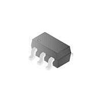
CNY173SM Fairchild Semiconductor, CNY173SM Datasheet

CNY173SM
Specifications of CNY173SM
Related parts for CNY173SM
CNY173SM Summary of contents
Page 1
... CEO White Package (-M Suffi Schematic ©2004 Fairchild Semiconductor Corporation CNY17-1, CNY17-3, CNY17-2, CNY17-4 Rev. 1.0.2 Applications ■ Power supply regulators ■ Digital logic inputs ■ Microprocessor inputs ■ Appliance sensor systems ■ Industrial controls Description The CNY17 series consists of a Gallium Arsenide IRED coupled with an NPN phototransistor. Black Package (No -M Suffi ...
Page 2
Parameters TOTAL DEVICE Storage Temperature Operating Temperature Lead Solder Temperature Total Device Power Dissipation @ 25°C (LED plus detector) Derate Linearly From 25°C EMITTER Continuous Forward Current Reverse Voltage Forward Current - Peak (1 µs pulse, 300 pps) LED Power ...
Page 3
Isolation Characteristics Characteristic Test Conditions Symbol Input-Output Isolation Voltage Hz min. Isolation Resistance V I-O Isolation Capacitance V I-O Note * 5300 Vac(rms) for 1 minute equates to approximately 9000 Vac (pk) for 1 ...
Page 4
Transfer Characteristics DC Characteristics Fall-Time (Fig. 19 and Fig. 20 Storage Time (Fig. 19 and Fig. I 20) I CNY17-1, CNY17-3, CNY17-2, CNY17-4 Rev. 1.0 25°C Unless otherwise specified.) (Continued) A Test Conditions Symbol ...
Page 5
Fig.1 Normalized CTR vs. Forward Current (Black Package 25˚C A 1.2 1.0 0.8 0.6 0.4 0.2 0 FORWARD CURRENT (mA) F Fig. 3 Normalized CTR vs. Ambient Temperature ...
Page 6
Fig. 7 CTR vs. RBE (Saturated) (Black Package) 1.0 0.9 0.8 0.7 0.6 0.5 0.4 0.3 0.2 0.1 0.0 10 100 - BASE RESISTANCE (k Ω Fig. 9 Switching Speed vs. Load Resistor (Black Package) 1000 I = ...
Page 7
Fig. 13 Normalized t (Black Package) 1.4 1.3 1.2 1.1 1.0 0.9 0.8 0.7 0.6 0.5 0.4 0.3 0.2 0.1 10 100 1000 - BASE RESISTANCE (k Ω Fig. 15 LED Forward Voltage vs. Forward Current (Black Package) ...
Page 8
INPUT Figure 19. Switching Time Test Circuit CNY17-1, CNY17-3, CNY17-2, CNY17-4 Rev. 1.0 10 90% OUTPUT ( Figure 20. Switching Time Test Circuit 8 ...
Page 9
Black Package (No -M Suffix) Package Dimensions (Through Hole) PIN 1 ID. 0.270 (6.86) 0.240 (6.10) 0.350 (8.89) 0.330 (8.38) 0.070 (1.78) 0.045 (1.14) 0.200 (5.08) 0.115 (2.92) 0.020 (0.51) 0.154 (3.90) MIN 0.100 (2.54) 0.016 (0.40) 0.008 (0.20) 0.022 ...
Page 10
White Package (-M Suffix) Package Dimensions (Through Hole) 0.350 (8.89) 0.320 (8.13) Pin 1 ID 0.260 (6.60) 0.240 (6.10) 0.070 (1.77) 0.040 (1.02) 0.014 (0.36) 0.010 (0.25) 0.200 (5.08) 0.115 (2.93) 0.100 (2.54) 0.015 (0.38) 0.020 (0.50) 0.100 (2.54) 0.016 ...
Page 11
Ordering Information Black Package Option (No Suffi 300 300W .300W 3S 3SD .3SD Carrier Tape Specifications (Black Package, No Suffix) 4.85 ± 0.20 0.30 ± 0.05 13.2 ± 0.2 0.1 MAX Carrier Tape Specifications (White Package, -M ...
Page 12
Marking Information Definitions Reflow Profile (Black Package, No Suffix) 300 250 225 C peak 200 150 100 Time above 183° C, 60–150 sec 50 Ramp C/sec 0 0 0.5 1 1.5 ...
Page 13
Reflow Profile (White Package, -M Suffix) 300 280 260 240 220 200 180 160 °C 140 120 100 CNY17-1, CNY17-3, CNY17-2, CNY17-4 Rev. 1.0.2 260°C Time above 183° Sec 1.822°C/Sec Ramp up ...
Page 14
... TRADEMARKS The following are registered and unregistered trademarks Fairchild Semiconductor owns or is authorized to use and is not intended exhaustive list of all such trademarks. FAST ACEx™ ActiveArray™ FASTr™ Bottomless™ FPS™ Build it Now™ FRFET™ CoolFET™ ...


