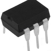
4N32M Fairchild Semiconductor, 4N32M Datasheet - Page 4

4N32M
Manufacturer Part Number
4N32M
Description
Transistor Output Optocouplers Optocoupler Photodarlington
Manufacturer
Fairchild Semiconductor
Datasheet
1.4N33M.pdf
(10 pages)
Specifications of 4N32M
Maximum Input Diode Current
80 mA
Maximum Reverse Diode Voltage
3 V
Output Device
Darlington With Base
Output Type
DC
Configuration
1
Input Type
DC
Maximum Collector Emitter Voltage
30 V
Maximum Collector Emitter Saturation Voltage
1000 mV
Isolation Voltage
5300 Vrms
Maximum Forward Diode Voltage
1.5 V
Maximum Collector Current
150 mA
Maximum Power Dissipation
250 mW
Maximum Operating Temperature
+ 100 C
Minimum Operating Temperature
- 40 C
Package / Case
PDIP White
Number Of Elements
1
Reverse Breakdown Voltage
3V
Forward Voltage
1.5V
Forward Current
80mA
Collector-emitter Voltage
30V
Package Type
PDIP W
Collector Current (dc) (max)
150mA
Power Dissipation
250mW
Collector-emitter Saturation Voltage
1V
Pin Count
6
Mounting
Through Hole
Operating Temp Range
-40C to 100C
Operating Temperature Classification
Industrial
Lead Free Status / RoHS Status
Lead free / RoHS Compliant
Available stocks
Company
Part Number
Manufacturer
Quantity
Price
Part Number:
4N32M
Manufacturer:
FAIRCHILD/ن»™ç«¥
Quantity:
20 000
©2007 Fairchild Semiconductor Corporation
4NXXM, H11B1M, TIL113M Rev. 1.0.3
Electrical Characteristics
Isolation Characteristics
* Indicates JEDEC registered data.
Notes:
1. The current transfer ratio(I
2. Pulse test: pulse width = 300µs, duty cycle
3. I
4. The frequency at which I
5. For this test, LED pins 1 and 2 are common, and phototransistor pins 4, 5 and 6 are common.
Safety and Insulation Ratings
As per IEC 60747-5-2, this optocoupler is suitable for “safe electrical insulation” only within the safety limit data.
Compliance with the safety ratings shall be ensured by means of protective circuits.
Symbol
Symbol
F
V
R
C
V
V
adjusted to I
V
RIO
CTI
ISO
IORM
ISO
ISO
IOTM
PR
Input-Output Isolation Voltage
Isolation Resistance
Isolation Capacitance
Installation Classifications per DIN VDE 0110/1.89
Table 1
For Rated Main Voltage < 150Vrms
For Rated Main voltage < 300Vrms
Climatic Classification
Pollution Degree (DIN VDE 0110/1.89)
Comparative Tracking Index
Input to Output Test Voltage, Method b,
V
with tm = 1 sec, Partial Discharge < 5pC
Input to Output Test Voltage, Method a,
V
with tm = 60 sec, Partial Discharge < 5pC
Max. Working Insulation Voltage
Highest Allowable Over Voltage
External Creepage
External Clearance
Insulation Thickness
Insulation Resistance at Ts, V
IORM
IORM
C
= 2.0mA and I
Characteristic
x 1.875 = V
x 1.5 = V
C
C
is 3dB down from the 1kHz value.
/I
PR
F
(5)
) is the ratio of the detector collector current to the LED input current.
PR
, Type and Sample Test
C
(5)
Parameter
= 0.7mA rms.
, 100% Production Test
(T
A
= 25°C Unless otherwise specified.) (Continued)
(5)
IO
f = 60Hz, t = 1 sec.
VDC
VDC
V
V
I-O
I-O
= 500V
2.0% .
Test Conditions
= 500VDC
= Ø, f = 1MHz
4
Min.
1594
1275
6000
175
850
10
0.5
4N32M*
4N33M*
Device
7
7
9
All
All
All
55/100/21
Min.
7500
2500
1500
Typ.
10
I-IV
I-IV
2
11
Typ.
0.8
Max.
Max.
www.fairchildsemi.com
V
AC
Units
V
V
V
V
Unit
mm
mm
mm
pF
PEAK
peak
peak
peak
peak
V


