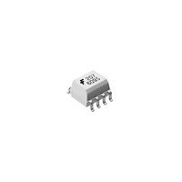
FOD2742B Fairchild Semiconductor, FOD2742B Datasheet - Page 3

FOD2742B
Manufacturer Part Number
FOD2742B
Description
Transistor Output Optocouplers Error amplifier Optocoupler
Manufacturer
Fairchild Semiconductor
Specifications of FOD2742B
Maximum Input Diode Current
20 mA
Output Device
Transistor
Output Type
DC
Configuration
1
Input Type
DC
Maximum Collector Emitter Voltage
70 V
Maximum Collector Emitter Saturation Voltage
400 mV
Isolation Voltage
2500 Vrms
Current Transfer Ratio
200 %
Maximum Forward Diode Voltage
1.5 V
Maximum Collector Current
50 mA
Maximum Power Dissipation
145 mW
Maximum Operating Temperature
+ 85 C
Minimum Operating Temperature
- 25 C
Package / Case
SOIC-8 Narrow
No. Of Channels
1
Optocoupler Output Type
Phototransistor
Input Current
10mA
Output Voltage
70V
Opto Case Style
SOIC
No. Of Pins
8
Svhc
No SVHC (15-Dec-2010)
Rohs Compliant
Yes
Lead Free Status / RoHS Status
Lead free / RoHS Compliant
Other names
FOD2742B_NL
Available stocks
Company
Part Number
Manufacturer
Quantity
Price
Part Number:
FOD2742B
Manufacturer:
FAIRCHILD/ن»™ç«¥
Quantity:
20 000
Company:
Part Number:
FOD2742BR2
Manufacturer:
FAIRCHIL
Quantity:
2 671
© 2003 Fairchild Semiconductor Corporation
FOD2742A
1. The deviation parameters V
2. The dynamic impedance is defined as |Z
ELECTRICAL CHARACTERISTICS
INPUT CHARACTERISTICS
Parameter
LED Forward Voltage
Reference Voltage
Deviation of V
temperature
Ratio of V
output of the error amplifier
Feedback Input Current
Deviation of I
temperature
Minimum Drive Current
Off-state error amplifier current
Error amplifier output impedance
(see note 2)
Z
∆V
obtained over the rated temperature range. The average full-range temperature coefficient of the reference input voltage, ∆ V
is defined as:
where ∆ T
(see Figure 2), the total dynamic impedance of the circuit is given by:
OUT, TOT
REF
(
REF
ppm/°C
A
=
is the rated operating free-air temperature range of the device.
REF
REF
variation to the
∆V
------- -
∆I
over
)
≈
over
=
Z
OUT
{
---------------------------------------------------------------------------------------------------- -
V
REF DEV
×
(
REF(DEV)
1
+
)
R1
------- -
R2
/V
I
LED
REF
V
(I
and I
COMP
∆T
LED
I
LED
= 10 mA
(
T
I
A
OUT
(fig. 2)
LED
A
= 10 mA, V
REF(DEV)
= 10 mA, V
=
= V
| = ∆ V
T
T
= 10mA, R
V
25°C
A
A
LED
REF
(T
= -25°C to +85°C (fig. 1) V
= -25°C to +85°C (fig. 3)
∆ V
FOD2742B
, I
A
∆ V
)
COMP
= 37V, V
are defined as the differences between the maximum and minimum values
} 10
LED
V
= 25°C Unless otherwise specified.)
COMP
COMP
COMP
×
COMP
COMP
Test Conditions
Page 3 of 13
/ ∆ I
1
= 1mA to 20mA,
6
= 10K Ω (fig. 3)
= 10V to V
LED
= V
FB
= 36V to 10V
= V
= V
f ≥ 1.0 kHz
. When the device is operating with two external resistors
= 0 (fig. 4)
FB
FB
FB
) (fig. 1)
(fig. 1)
(fig. 1)
REF
I
I
REF (DEV)
Symbol
∆ V
LED (MIN)
REF (DEV)
∆ V
|Z
I
V
OPTICALLY ISOLATED
I
(OFF)
REF
V
COMP
OUT
REF
REF
F
|
/
ERROR AMPLIFIER
Device
ALL
ALL
ALL
ALL
ALL
ALL
ALL
ALL
C
A
B
2.482 2.495 2.508
2.470 2.495 2.520
2.450 2.500 2.550
Min.
FOD2742C
1.20
0.45
0.01
0.15
Typ.
-0.5
-0.3
3.5
2.2
1.0
Max.
-2.7
-2.0
1.5
1.2
1.0
1.0
0.5
17
4
12/9/04
Unit
mV/
mV
mA
µA
µA
µA
REF
Ω
V
V
V
V
V
,


