VNCLO-SHLD-1A FTDI, VNCLO-SHLD-1A Datasheet - Page 16
VNCLO-SHLD-1A
Manufacturer Part Number
VNCLO-SHLD-1A
Description
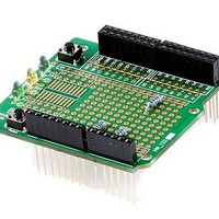
Interface Modules & Development Tools Vinculo Prototyping Shield Accessory
Manufacturer
FTDI
Datasheet
1.VNCLO-MB1A.pdf
(26 pages)
Specifications of VNCLO-SHLD-1A
Interface Type
USB, Serial, UART, FIFO, SPI
Data Bus Width
Serial, 8 bit
Operating Supply Voltage
100 VAC to 240 VAC
Product
Interface Development Tools
Features
Precompiled Drivers For A Variety Of Interfaces
Kit Contents
Board
Kit Features
Precompiled Drivers, Compatible With Existing Shields
Mcu Supported Families
VNC2
Silicon Family Name
Vinculum
For Use With/related Products
VNC2
Lead Free Status / RoHS Status
Lead free / RoHS Compliant


5
The purpose of the debugger interface, J8, is to provide access to the VNC2 silicon/firmware debugger.
The debug interface can be accessed by connecting a VNC2_Debugger_Programmer_Module to the J8
connector. This debugger/programmer module will give access to the debugger through a USB connection
to a PC via the Integrated Development Environment (IDE). The IDE is accessed through a GUI to the
VNC2 software development tool-chain and gives the following debug capabilities through the debugger
interface:
The IDE may be downloaded from
The Debugger Interface, and how to use it, is further described in the following applications note:
Vinculum-II Debug Interface
5.1 Signal Description - Debugger Interface
Table 5.1 shows the signals and pins description for the Debugger Interface pin header J8
Table 5.1 – Signal Name and Description – Debugger Interface
Note: # defines active low signals.
Pin No.
J7-1
J7-2
J7-3
J7-4
J7-5
J7-6
Debugger Interface
Flash Erase, Write and Program.
Application debug - application code can have breakpoints, be single stepped and can be halted.
Detailed internal debug - memory and register read/write access.
RESET#
PROG#
Name
GND
IO0
5V0
-
Copyright © 2010-2011 Future Technology Devices International Limited
On PCB
Name
PRG#
[Key]
RST#
DBG
GND
VCC
Description.
http://www.ftdichip.com/Firmware/V2TC/VNC2toolchain.htm
PWR Input
Type
Input
Input
PWR
I/O
-
Debugger Interface
Not connected. Used to make sure that the debug
module is connected correctly.
Module ground supply pin
Can be used by an external device to reset the
VNC2. This pin is also used in combination with
PROG# and the UART interface to program
firmware into the VNC2.
This pin is used in combination with the RESET#
pin and the UART interface to program firmware
into the VNC2.
5.0V module supply pin. This pin can be used to
provide the 5.0V input to the Vinco from the
debugger interface when the Vinco is not powered
from the USB connector (VBUs) or the CN1
Vinco Development Module Datasheet Version 2.0
Document Reference No.: FT_000327
Description
Clearance No.: FTDI#173
12
Related parts for VNCLO-SHLD-1A
Image
Part Number
Description
Manufacturer
Datasheet
Request
R

Part Number:
Description:
POWER SUPPLY FOR VNCLO-MB1A USA
Manufacturer:
FTDI, Future Technology Devices International Ltd
Datasheet:

Part Number:
Description:
POWER SUPPLY FOR VNCLO-MB1A EU
Manufacturer:
FTDI, Future Technology Devices International Ltd
Datasheet:
Part Number:
Description:
POWER SUPPLY FOR VNCLO-MB1A UK
Manufacturer:
FTDI, Future Technology Devices International Ltd
Datasheet:

Part Number:
Description:
Interface Modules & Development Tools Vinculo Motherboard Req VNC2DEBUGMODULE
Manufacturer:
FTDI
Datasheet:
Part Number:
Description:
KIT, DEV, VINCULUM-II, VNC2
Manufacturer:
FTDI
Datasheet:
Part Number:
Description:
BOARD, EVALUATION, US PSU
Manufacturer:
FTDI
Datasheet:
Part Number:
Description:
Specifications: Manufacturer: FTDI ; Product Category: USB Interface IC ; RoHS: Details ; Operating Supply Voltage: 3 V to 5.25 V ; Supply Current: 25 mA ; Maximum Operating Temperature: + 70 C ; Mounting Style: SMD/SMT ; Package / Case: QFN-32
Manufacturer:
FTDI

Part Number:
Description:
IC USB TO SERIAL UART 32-QFN
Manufacturer:
FTDI, Future Technology Devices International Ltd

Part Number:
Description:
USB Interface IC USB to Serial UART Enhanced IC SSOP-28
Manufacturer:
FTDI
Datasheet:

Part Number:
Description:
IC, USB UART INTERFACE, SSOP-28
Manufacturer:
FTDI
Datasheet:

Part Number:
Description:
IC, USB UART INTERFACE, QFN-32
Manufacturer:
FTDI
Datasheet:
Part Number:
Description:
IC, USB FIFO INTERFACE, SSOP-28
Manufacturer:
FTDI
Datasheet:
Part Number:
Description:
MODULE, USB, 4 PORT, FT4232H BASED
Manufacturer:
FTDI
Datasheet:
Part Number:
Description:
357-036-542-201 CARDEDGE 36POS DL .156 BLK LOPRO
Manufacturer:
FTDI
Datasheet:
Part Number:
Description:
357-036-542-201 CARDEDGE 36POS DL .156 BLK LOPRO
Manufacturer:
FTDI
Datasheet: