CDB1600-120W Cirrus Logic Inc, CDB1600-120W Datasheet - Page 9
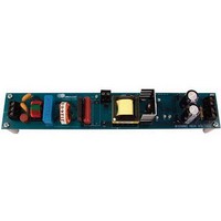
CDB1600-120W
Manufacturer Part Number
CDB1600-120W
Description
Power Management Modules & Development Tools Dev Board for CS1600
Manufacturer
Cirrus Logic Inc
Type
Power Factor Correctionr
Specifications of CDB1600-120W
Input Voltage
108 VAC to 305 VAC
Output Voltage
460 V
Board Size
223 mm x 38 mm
Output Power
120 W
Product
Power Management Modules
Dimensions
223 mm x 38 mm
Kit Contents
Board, Datasheet
Tool / Board Applications
Power Management-Voltage/Current Regulation, PFC, Power Supply
Development Tool Type
Hardware - Eval/Demo Board
Mcu Supported Families
CS1600
For Use With/related Products
CS1600
Lead Free Status / RoHS Status
Lead free / RoHS Compliant


5.4 Output Power and PFC Boost Inductor
In normal operating mode, the nominal output power is
estimated by the following equation.
where:
P
V
V
f
L
Equation 1 is provided for explanation purposes only. Using
substituted required design values for V
following equation.
Changing values for application-specific devices such as the
boost inductor or V
requires changing internal register values.
Solving Equation 2 for the PFC boost inductor L
following equation.:
If a value of the boost inductor other than that obtained from
Equation 3 above is used, the total output power capability as
well as the minimum input voltage threshold will differ
according to Equation 2.
DS904F1
max
Figure 15. Relative Effects of Varying Boost Inductance
B
o
in(min)
link
P
L
P
o
o
B
=
=
=
by the PFC algorithm)
against boost inductor tolerances.
rated output power of the system
efficiency of the boost converter (estimated as 100%
minimum RMS line voltage is 108V, measured after
the rectifier and EMI filter
nominal PFC output voltage must be 460 V
maximum switching frequency is 70 kHz
boost inductor specified by rated power requirement
margin factor to guarantee rated output power (P
V
108V
108V
in min
108
link
2
2
voltage is not recommended and
2
------------------------------------------------------------ -
2 70kHz P
V
------------------------------------------------------------ -
2 70kHz
460V
AC(rms)
460V
V
-------------------------------------------------------- -
2 f
link
L < L
L > L
–
–
max
–
L = L
108V
V
108V
in min
B
B
link
B
L
o
L
B
B
and f
460V
460V
V
2
2
link
max
2
305
B
gives the
gives the
[Eq.1]
[Eq.2]
[Eq.3]
o
)
5.5 PFC Output Capacitor
The value of the PFC output capacitor should be chosen
based upon voltage ripple and hold-up requirements. To
ensure system stability with the digital controller, the
recommended value of the capacitor is within the range of
0.25 F / watt to 0.5 F / watt.
5.6 Output IFB Sense & Input IAC Sense
A current proportional to the PFC output voltage, V
supplied to the IC on pin IFB and is used as a feedback control
signal. This current is compared against an internal fixed-
value current.
The ADC is used to measure the magnitude of the I
through resistor R
compared to an internal fixed-value current.
Resistor R
follows:
By using digital loop compensation, the voltage feedback
signal does not require an external compensation network.
A current proportional to the AC input voltage is supplied to the
IC on pin IAC and is used by the PFC control algorithm.
Resistor R
For optimal performance, resistors R
tolerance or better resistors.
IAC
Figure 16. Feedback Input Pin Model
IFB
V
I
R
I
FB
rec t
AC
Figure 17. IAC Input Pin Model
sets the IAC current and is derived as follows:
sets the feedback current and is calculated as
IFB
IFB
=
. The magnitude of the I
R3
R4
V
--------------------------- -
R1
R2
link
R
I
R
fixed
R
IFB
IAC
IA C
IFB
–
IAC
V
4
3
dd
=
R
=
IFB
7
7
15k
V
15k
V DD
460V V
----------------------------- -
IAC
V DD
24k
24k
link
129 A
& R
–
IFB
CS1600
FB
CS1600
ADC
dd
ADC
should use 1%
CS1600
current is then
FB
current
[Eq.4]
link
[Eq.5]
, is
9
Related parts for CDB1600-120W
Image
Part Number
Description
Manufacturer
Datasheet
Request
R

Part Number:
Description:
DEVELOPMENT BOARD FOR CS1600
Manufacturer:
Cirrus Logic Inc
Datasheet:

Part Number:
Description:
Development Kit
Manufacturer:
Cirrus Logic Inc
Datasheet:
Part Number:
Description:
Development Kit
Manufacturer:
Cirrus Logic Inc
Datasheet:


Part Number:
Description:
High-efficiency PFC + Fluorescent Lamp Driver Reference Design
Manufacturer:
Cirrus Logic Inc
Datasheet:
Part Number:
Description:
Development Kit
Manufacturer:
Cirrus Logic Inc
Datasheet:
Part Number:
Description:
Development Kit
Manufacturer:
Cirrus Logic Inc
Datasheet:

Part Number:
Description:
Development Kit
Manufacturer:
Cirrus Logic Inc
Datasheet:
Part Number:
Description:
Development Kit
Manufacturer:
Cirrus Logic Inc
Datasheet:
Part Number:
Description:
Development Kit
Manufacturer:
Cirrus Logic Inc
Datasheet:

Part Number:
Description:
EVALUATION BOARD FOR CS8427
Manufacturer:
Cirrus Logic Inc
Datasheet:

Part Number:
Description:
BOARD EVAL FOR CS8416 RCVR
Manufacturer:
Cirrus Logic Inc
Datasheet:

Part Number:
Description:
EVALUATION BOARD FOR CS8420
Manufacturer:
Cirrus Logic Inc
Datasheet:

Part Number:
Description:
KIT DEVELOPMENT EP9315 ARM9
Manufacturer:
Cirrus Logic Inc
Datasheet:

Part Number:
Description:
KIT DEVELOPMENT EP9302 ARM9
Manufacturer:
Cirrus Logic Inc
Datasheet: