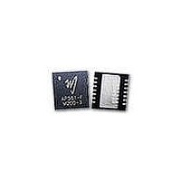
AP561-PCB2500 TriQuint, AP561-PCB2500 Datasheet - Page 10

AP561-PCB2500
Manufacturer Part Number
AP561-PCB2500
Description
WiFi / 802.11 Modules & Development Tools 2.4-2.7GHz Eval Brd 1W 12V
Manufacturer
TriQuint
Datasheet
1.AP561-PCB2500.pdf
(15 pages)
Specifications of AP561-PCB2500
Wireless Frequency
2.5 GHz to 2.7 GHz
Board Size
5 mm x 6 mm
Modulation
OFDMA
Operating Voltage
12 V
Output Power
1 W
For Use With/related Products
AP561
Lead Free Status / RoHS Status
Lead free / RoHS Compliant
Other names
1067303
Available stocks
Company
Part Number
Manufacturer
Quantity
Price
Part Number:
AP561-PCB2500
Manufacturer:
WJ
Quantity:
20 000
TriQuint Semiconductor Inc • Phone +1-503-615-9000 • FAX: +1-503-615-8900 • e-mail: info-sales@tqs.com • Web site: www.TriQuint.com
AP561
0.7-2.9 GHz 8W Power Amplifier
Frequency (GHz)
Channel Power
Power Gain
Input Return Loss
Output Return Loss
EVM
Operating Current, Icc 510
Collector Efficiency 15.8 17.6
Output P1dB
Quiescent Current Icq
Reference Current Iref
Vpd
Vcc
Typical O-FDMA Performance at 25°C
14
13
12
11
10
9
8
7
6
5
4
9
2.4
2.4
802.16-2004 O-FDMA, 64QAM-1/2, 1024-FFT, 20 symbols and 30 subchannels. 9.5 dB PAR @ 0.01%, 5 MHz Carrier BW
- 40C
2.5
2.5
25C
NF vs. Frequency
Gain vs. Frequency
Frequency (GHz)
Frequency (GHz)
Freq = 2.6GHz
13.4 13.1
39.7 39.0
+30
2.5
6.4
2.2
12
+ 85C
T=25°C
2.5-2.7 GHz Application Circuit Performance Plots
2.5-2.7 GHz Application Circuit (AP561-PCB2500)
2.6
2.6
+30
480
2.6
6.2
1.5
300
+12
13
+5
10
2.7
2.7
12.2
37.6
+30
490
2.7
4.3
2.1
16
16
Units
dBm
dBm
mA
mA
mA
dB
dB
dB
%
%
V
V
2.8
2.8
14
13
12
11
10
-10
-15
-20
-5
0
24
2.4
Notes:
1.
2.
3.
4.
5.
6.
7.
8.
9.
10. 0 Ω jumpers can be replaced with copper trace in target application.
Power Gain vs. Output Average Power vs. Vcc
26
The primary RF microstrip line is 50 Ω.
Do not exceed 5.5V on Vpd or damage to D1 will occur.
Do not exceed 13V on Vcc or damage to D2 will occur.
Components shown on the silkscreen but not on the schematic are not used.
The edge of C23 is placed right next to C24.
The edge of C24 is placed at 85mil from AP561 RFout pin. (9.6
The edge of C25 is placed at 56mil from AP561 RFin pin. (6.3
The edge of C26 is placed right next to C25.
The edge of C27 is placed 55mil from the edge of C26. (6.2
28
2.5
Return Loss vs. Frequency
+8V
+12V
Frequency (GHz)
Output Power (dBm)
30
Freq = 2.6GHz
T=25°C
2.6
32
+10V
+14V
34
2.7
36
S11
38
S22
2.8
40
Specifications and information are subject to change without notice
14
13
12
11
10
42
40
38
36
34
32
9
2.4
2.4
Power Gain vs.Frequency vs. Vcc
2.5
2.5
+8V
P1dB vs. Frequency
T = 25C, Icq = 300mA
o
+25C
Frequency (GHz)
Frequency (GHz)
@ 2.6 GHz)
+10V
o
o
@ 2.6 GHz)
@ 2.6 GHz)
2.6
2.6
-40C
+12V
Page 10 of 15 April 2010
+85C
+14V
2.7
2.7
2.8
2.8


