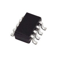
MAX9615AXA+T Maxim Integrated Products, MAX9615AXA+T Datasheet - Page 2

MAX9615AXA+T
Manufacturer Part Number
MAX9615AXA+T
Description
Op Amps LW-POW SNGL/DUAL R-R I/O OP AMPS
Manufacturer
Maxim Integrated Products
Datasheet
1.MAX9613EVKIT.pdf
(12 pages)
Specifications of MAX9615AXA+T
Number Of Channels
2
Common Mode Rejection Ratio (min)
80 dB
Input Voltage Range (max)
5.5 V
Input Voltage Range (min)
1.8 V
Input Offset Voltage
23 uV
Input Bias Current (max)
135 pA
Supply Current
220 uA
Maximum Power Dissipation
245 mW
Maximum Operating Temperature
+ 125 C
Minimum Operating Temperature
- 40 C
Mounting Style
SMD/SMT
Slew Rate
1.3 V/us
Package / Case
SC70-8
Lead Free Status / RoHS Status
Lead free / RoHS Compliant
Low-Power, High-Efficiency,
Single/Dual, Rail-to-Rail I/O Op Amps
ABSOLUTE MAXIMUM RATINGS
IN+, IN-, SHDN, V
OUT to GND ............................................. -0.3V to (V
Short-Circuit (GND) Duration to Either Supply Rail ................. 5s
Continuous Input Current (any pin) ................................. Q20mA
Thermal Limits (Note 1) Multilayer PCB
Continuous Power Dissipation (T
Note 1: Package thermal resistances were obtained using the method described in JEDEC specification JESD51-7, using a four-
ELECTRICAL CHARACTERISTICS
(V
otherwise noted.) (Note 2)
Stresses beyond those listed under “Absolute Maximum Ratings” may cause permanent damage to the device. These are stress ratings only, and functional
operation of the device at these or any other conditions beyond those indicated in the operational sections of the specifications is not implied. Exposure to absolute
maximum rating conditions for extended periods may affect device reliability.
2
DC CHARACTERISTICS
Input Voltage Range
Input Offset Voltage
Input Offset Voltage Drift
Input Bias Current (Note 3)
Common-Mode Rejection Ratio
Input Offset Current (Note 3)
Open-Loop Gain
Output Short-Circuit Current
(Note 4)
Output Voltage Low
CC
6-Pin SC70 (derate 3.1mW/NC above +70NC) .............245mW
______________________________________________________________________________________
B
B
JA
JC
= V
.......................................................................326.5NC/W
..........................................................................115NC/W
layer board. For detailed information on package thermal considerations, refer to www.maxim-ic.com/thermal-tutorial.
SHDN
PARAMETER
= 3.3V, V
CC
to GND..................................-0.3V to +6V
IN+
= V
IN-
A
= +70NC)
= V
V
SYMBOL
V
CM
IN+
CMRR
OS
V
A
V
I
I
OS
I
SC
OS
OL
OL
, V
B
= 0V, R
- TC
IN-
Guaranteed by CMRR test
T
T
calibration
T
T
T
T
T
V
V
+125NC
T
T
T
T
+0.4V P V
To V
To GND
R
R
R
L
A
A
A
A
A
A
A
A
A
A
A
CM
CM
L
L
L
= 10kI to V
CC
= +25NC
= -40NC to +125NC after power-up auto-
= -40NC to +125NC
= +40°C to +25°C
= +70°C
= +85°C
= +125°C
= +40°C to +25°C
= +70°C
= +85°C
= +125°C
= 10kI
= 600I
= 32I
CC
= -0.1V to V
= -0.1V to V
+ 0.3V)
OUT
CC
P V
CONDITIONS
/2, T
CC
CC
CC
Operating Temperature Range ........................ -40NC to +125NC
Storage Temperature Range ............................ -65NC to +150NC
Junction Temperature .....................................................+150NC
Lead Temperature (soldering, 10s) ................................+300NC
Soldering Temperature (reflow) ......................................+260NC
+ 0.1V, T
+ 0.1V, T
A
- 0.4V, R
8-Pin SC70 (derate 3.1mW/NC above +70NC) .............245mW
= -40NC to +125NC. Typical values are at T
B
B
JA
JC
.......................................................................... 326NC/W
..........................................................................115NC/W
A
A
L
= +25NC
= -40NC to
= 10kI
MIN
-0.1
82
80
99
0.170
TYP
100
120
275
23
75
1
1
A
V
0.011
MAX
1.55
1.55
135
400
CC
100
150
750
0.1
0.5
0.1
= +25NC, unless
45
25
7
7
+
UNITS
FV/NC
mA
pA
nA
dB
pA
dB
FV
V
V


