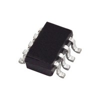
MAX9616AXA+T Maxim Integrated Products, MAX9616AXA+T Datasheet - Page 9

MAX9616AXA+T
Manufacturer Part Number
MAX9616AXA+T
Description
Op Amps LW-POW SNGL/DUAL R-R I/O OP AMPS
Manufacturer
Maxim Integrated Products
Datasheet
1.MAX9614AXTT.pdf
(12 pages)
Specifications of MAX9616AXA+T
Number Of Channels
2
Common Mode Rejection Ratio (min)
78 dB
Input Voltage Range (max)
5.5 V
Input Voltage Range (min)
2.5 V
Input Offset Voltage
17 uV
Input Bias Current (max)
135 pA
Supply Current
170 uA
Maximum Power Dissipation
245 mW
Maximum Operating Temperature
+ 125 C
Minimum Operating Temperature
- 40 C
Mounting Style
SMD/SMT
Slew Rate
1.3 V/us
Package / Case
SC70-8
Lead Free Status / RoHS Status
Lead free / RoHS Compliant
The MAX9614/MAX9616 feature a high-impedance
CMOS input stage and a specialized ESD structure
that allows low input bias current operation at low
input common-mode voltages. Low input bias current
is useful when interfacing with high-ohmic sensors. It
is also beneficial for designing transimpedance ampli-
fiers for photodiode sensors. This makes the MAX9614/
MAX9616 ideal for ground referenced medical and
industrial sensor applications.
Low-Power Single/Dual, Rail-to-Rail Op Amps
_______________________________________________________________________________________
Input Bias Current
PROCESS: BiCMOS
The MAX9614/MAX9616 are ideal for a wide variety
of active filter circuits that make use of their rail-to-rail
output stages and high impedance CMOS inputs. The
Typical Application Circuit shows an example multiple
feedback active filter circuit with a corner frequency
of 1.3kHz. At low frequencies, the amplifier behaves
like a simple low-distortion inverting amplifier of gain =
-1, while its high bandwidth gives excellent stopband
attenuation above its corner frequency. See the Typical
Application Circuit.
Chip Information
Active Filters
9


