BGA 428 H6327 Infineon Technologies, BGA 428 H6327 Datasheet
BGA 428 H6327
Specifications of BGA 428 H6327


Related parts for BGA 428 H6327


BGA 428 H6327 Summary of contents
Page 1
...
Page 2
... Infineon Technologies Office. Infineon Technologies Components may only be used in life-support devices or systems with the express written approval of Infineon Technologies failure of such components can reasonably be expected to cause the failure of that life-support device or system affect the safety or effectiveness of that device or system. Life support devices or systems are intended to be implanted in the human body support and/or maintain and sustain and/or protect human life ...
Page 3
... BGA428, Gain and PCS Low Noise Amplifier Revision History: 2007-11-06, Rev. 2.2 Previous Version: 2002-03-26 Page Subjects (major changes since last revision) 9 Correction of cross-reference Trademarks ® SIEGET is a registered trademark of Infineon Technologies AG. Data Sheet 3 BGA428 Rev. 2.2, 2007-11-06 ...
Page 4
Silicon Germanium Broadband MMIC Amplifier Feature G • High gain 1.8 GHz MA NF • Low noise figure 1.8 GHz • Prematched • Ideal for GSM, DCS1800, PCS1900 • Open collector ...
Page 5
Maximum Ratings Table 1 Maximum ratings Parameter Device voltage Voltage at pin Out Voltage at pin GS Current into pin In 1) Total device current 2) Input power T Total power dissipation, < 125 °C S Junction temperature Operating temperature ...
Page 6
Electrical Characteristics 2.1 Electrical characteristics at V Figure 2), = 2.7 V, Frequency = 1.8 GHz, unless otherwise specified CC Table 3 Electrical Characteristics Parameter Maximum available power gain Z Noise figure ( = 50 S Input power at ...
Page 7
Table 4 S-Parameter at 2.7 V (see Electrical Characteristics for conditions) Frequency S11 S11 [GHz] Mag Ang 0.100 0.6756 -31.7 0.200 0.5936 -53.6 0.300 0.5150 -71.4 0.400 0.4587 -86.6 0.600 0.4004 -110.7 0.800 0.3743 -129.1 1.000 0.3743 -143.0 1.200 0.3816 ...
Page 8
Application Circuit Characteristics (measured in test circuit specified in T Figure 3 °C, A specified Table 5 Application Circuit Characteristics Parameter Insertion power gain Z Noise figure ( = 50 S Input power gain ...
Page 9
Measured Parameters Refer to the application circuit given in 2 Power Gain |S21| =f( 2.7V, V =2.7V CC Out −5 −10 −15 −20 − Frequency [GHz] 2 Off−Gain ...
Page 10
Input Compression Point P −16.5 −17 −17.5 −18 −18.5 V =2.85V CC −19 −19.5 −20 1800 1850 1900 Frequency [MHz] 2 Insertion Gain | =2.7V, V =2.7V CC Out f=1800MHz ...
Page 11
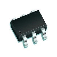
Package Information Pin 1 marking Figure 4 Package Outline SOT363 Figure 5 Tape for SOT363 Data Sheet 2 ±0.2 +0.1 6x 0.2 0.1 MAX. -0.05 0 0.65 0.65 0 ...