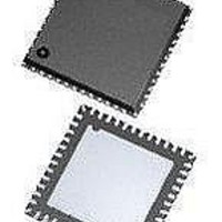
ASD5010L1000INT Arctic Silicon Devices, ASD5010L1000INT Datasheet - Page 17

ASD5010L1000INT
Manufacturer Part Number
ASD5010L1000INT
Description
ADC (A/D Converters) A-D Conv, Dig Gain Single 8 bit 1 GSPS
Manufacturer
Arctic Silicon Devices
Datasheet
1.ASD5010L500INT.pdf
(35 pages)
Specifications of ASD5010L1000INT
Number Of Converters
1
Number Of Adc Inputs
2
Conversion Rate
1000 MSPs
Resolution
8 bit
Snr
49.8 dB
Voltage Reference
1 V
Supply Voltage (max)
2 V
Supply Voltage (min)
1.7 V
Maximum Power Dissipation
710 mW
Maximum Operating Temperature
+ 85 C
Mounting Style
SMD/SMT
Package / Case
QFN-48
Input Voltage
1.8 V
Minimum Operating Temperature
- 40 C
Lead Free Status / RoHS Status
Lead free / RoHS Compliant
Preliminary Product Specification
Register Description
Software Reset
Setting the rst register bit to '1', restores the default value of all the internal registers including the rst register bit itself.
Modes of Operation and Clock divide factor
The ASD5010 has three main operating modes controlled by the register bits channel_num<2:0> as defined in table 6.
Power down mode, as described in section 'Startup Initialization', must be activated after or during a change of operating
mode to ensure correct operation. All active operating modes utilize interleaving to achieve high sampling speed. Quad
channel mode interleaves 2 ADC branches, dual channel mode interleaves 4 ADC branches, while single channel mode
interleave all 8 ADC branches.
Only one of the 3bits should be activated at the same time.
clk_divide<1:0> allows the user to apply an input clock frequency higher than the sampling rate. The clock divider will
divide the input clock frequency by a factor of 1, 2, 4, or 8, defined by the clk_divide<1:0> register. By setting the
clk_divide<1:0> value relative to the channel_num<2:0> value, the same input clock frequency can be used for all
settings on number of channels. e.g: When increasing the number of channels from 1 to 4, the maximum sampling rate is
reduced by a factor of 4. By letting clk_divide<1:0> follow the channel_num<2:0> value, and change it from 1 to 4, the
internal clock divider will provide the reduction of the sampling rate without changing the input clock frequency.
ASD5010
rst
channel_num <2:0> Set number of channels: 1, 2 or 4
clk_divide<1:0>
channel_num <2:0>
0
0
1
Name
Name
0
1
0
Self-clearing software reset.
channels.
Define clock divider factor: 1, 2, 4 or 8
1
0
0
clk_divide<1:0>
Description
Description
00 (default)
01
10
11
Mode of operation
Single channel
Quad channel
Dual channel
Table 7: Clock Divider Factor
Table 6: Modes of operation
Clock Divider Factor
rev 2.0, 2010.11.08
Divide by 1
4 channels
Default
Default
Inactive
Page 17 of 35
1
2
4
8
Quad channel where channel 1 corresponds to ADC1, channel2
D15 D14D13D12D11D10 D9 D8 D7 D6 D5 D4 D3 D2 D1 D0
D15 D14D13D12D11D10 D9 D8 D7 D6 D5 D4 D3 D2 D1 D0
Dual channel where channel 1 is made by interleaving ADC1
and ADC2, channel 2 by interleaving ADC3 and ADC4
to ADC2, channel3 to ADC3 and channel 4 to ADC4
Single channel by interleaving ADC1to ADC4
Input clock frequency / 1
Input clock frequency / 2
Input clock frequency / 4
Input clock frequency / 8
Sampling rate (FS)
X X
Description
X X X
Confidential
X
Address
Address
0x00
0x31
Hex
Hex


