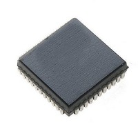
HV9708PJ-G Supertex, HV9708PJ-G Datasheet - Page 6

HV9708PJ-G
Manufacturer Part Number
HV9708PJ-G
Description
Serial to Parallel Logic Converters 80V 32Ch Hi-V Out
Manufacturer
Supertex
Datasheet
1.HV9708PJ-G.pdf
(7 pages)
Specifications of HV9708PJ-G
Input Bias Current (max)
0.1 mA
Logic Type
CMOS
Maximum Operating Temperature
+ 85 C
Minimum Operating Temperature
- 40 C
Mounting Style
SMD/SMT
Propagation Delay Time
110 ns @ 4.5 V to 5.5 V
Supply Voltage (max)
5.5 V
Supply Voltage (min)
4.5 V
Operating Supply Voltage
5 V
Package / Case
PLCC-44
Lead Free Status / RoHS Status
Lead free / RoHS Compliant
Available stocks
Company
Part Number
Manufacturer
Quantity
Price
Company:
Part Number:
HV9708PJ-G
Manufacturer:
Supertex
Quantity:
27
Pin Description
Pin
19
20
21
22
23
24
25
26
27
28
29
30
31
32
33
34
35
36
37
38
39
40
41
42
43
44
Latch Enable
Function
Blanking
HV
HV
HV
HV
HV
HV
HV
HV
HV
HV
HV
HV
HV
HV
HV
Polarity
Data In
GND
VDD
CLK
VPP
N/C
N/C
N/C
OUT
OUT
OUT
OUT
OUT
OUT
OUT
OUT
OUT
OUT
OUT
OUT
OUT
OUT
OUT
32
31
30
29
28
27
26
25
24
23
22
21
20
19
18
(cont.)
No connect.
---
Data shift register clock.
Input are shifted into the shift register on the positive edge of the clock.
Logic and high voltage ground.
High voltage power rail.
Low voltage logic power rail.
Latch enable input.
When LE is high, shift register data is transferred into a data latch. When LE is low, data is
latched, and new data can be clocked into the shift register.
Serial data input.
Data needs to be present before each rising edge of the clock.
---
No connect.
High voltage outputs.
High voltage push-pull outputs, which, depending on controlling low voltage data, can drive
loads either to a GND, or to V
PP
rail levels.
6
Function
HV9708


