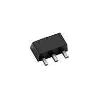
TN2510N8-G Supertex, TN2510N8-G Datasheet - Page 4

TN2510N8-G
Manufacturer Part Number
TN2510N8-G
Description
MOSFET Small Signal 100V 1.5Ohm
Manufacturer
Supertex
Type
Power MOSFETr
Datasheet
1.TN2510N8-G.pdf
(5 pages)
Specifications of TN2510N8-G
Minimum Operating Temperature
- 55 C
Configuration
Single
Transistor Polarity
N-Channel
Resistance Drain-source Rds (on)
1.5 Ohm @ 10 V
Drain-source Breakdown Voltage
100 V
Gate-source Breakdown Voltage
+/- 20 V
Continuous Drain Current
0.73 A
Power Dissipation
1600 mW
Maximum Operating Temperature
+ 150 C
Mounting Style
SMD/SMT
Package / Case
SOT-89
Number Of Elements
1
Polarity
N
Channel Mode
Enhancement
Drain-source On-res
1.5Ohm
Drain-source On-volt
100V
Gate-source Voltage (max)
±20V
Drain Current (max)
730mA
Output Power (max)
Not RequiredW
Frequency (max)
Not RequiredMHz
Noise Figure
Not RequireddB
Power Gain
Not RequireddB
Drain Efficiency
Not Required%
Operating Temp Range
-55C to 150C
Operating Temperature Classification
Military
Mounting
Surface Mount
Pin Count
2 +Tab
Package Type
SOT-89
Lead Free Status / RoHS Status
Lead free / RoHS Compliant
Typical Performance Curves
100
1.1
1.0
0.9
75
50
25
10
8
6
4
2
0
0
-50
0
0
Capacitance vs. Drain-to-Source Voltage
BV
V
GS
DSS
2
Transfer Characteristics
10
0
f = 1MHz
= 25V
Variation with Temperature
V
V
GS
4
DS
T
(volts)
j
50
20
° (
(volts)
C)
●
6
1235 Bordeaux Drive, Sunnyvale, CA 94089
100
30
8
(cont.)
C
C
RSS
ISS
150
10
40
4
1.2
1.1
1.0
0.9
0.8
10
10
8
6
4
2
0
8
6
4
2
0
-50
0
0
V
●
(th)
Gate Drive Dynamic Characteristics
Tel: 408-222-8888
70pF
On-Resistance vs. Drain Current
and R
0.5
2
0
DS
Q (nanocoulombs)
V
V
GS
G
(th)
I
D
Variation with Temperature
1.0
(amperes)
= 5V
@ 1mA
4
V
T
DS
j
50
R
° (
DS(ON)
C)
= 10V
●
1.5
6
190 pF
www.supertex.com
V
GS
@ 5V, 0.75A
V
100
DS
= 10V
2.0
8
= 40V
150
2.5
10
2.0
1.6
1.2
0.8
0.4
TN2510


