VP3203N3-G Supertex, VP3203N3-G Datasheet

MOSFET Small Signal 30V 0.6Ohm

VP3203N3-G

Manufacturer Part Number
VP3203N3-G
Description
MOSFET Small Signal 30V 0.6Ohm
Manufacturer
Supertex
Type
Power MOSFETr
Datasheet

Specifications of VP3203N3-G

Minimum Operating Temperature
- 55 C
Configuration
Single
Transistor Polarity
P-Channel
Resistance Drain-source Rds (on)
0.6 Ohm @ 10 V
Drain-source Breakdown Voltage
30 V
Gate-source Breakdown Voltage
+/- 20 V
Continuous Drain Current
0.65 A
Power Dissipation
740 mW
Maximum Operating Temperature
+ 150 C
Mounting Style
Through Hole
Package / Case
TO-92
Number Of Elements
1
Polarity
P
Channel Mode
Enhancement
Drain-source On-res
0.6Ohm
Drain-source On-volt
30V
Gate-source Voltage (max)
±20V
Operating Temp Range
-55C to 150C
Operating Temperature Classification
Military
Mounting
Through Hole
Pin Count
3
Package Type
TO-92
Lead Free Status / RoHS Status
Lead free / RoHS Compliant
Features
Applications
Ordering Information
-G indicates package is RoHS compliant (‘Green’)
* Mil visual screening available.
Absolute Maximum Ratings
Absolute Maximum Ratings are those values beyond which damage to the device
may occur. Functional operation under these conditions is not implied. Continuous
operation of the device at the absolute rating level may affect device reliability. All
voltages are referenced to device ground.
*
Parameter
Drain-to-source voltage
Drain-to-gate voltage
Gate-to-source voltage
Operating and storage temperature
Soldering temperature*
Distance of 1.6mm from case for 10 seconds.
Device
VP3203
Free from secondary breakdown
Low power drive requirement
Ease of paralleling
Low C
High input impedance and high gain
Excellent thermal stability
Integral source-to-drain diode
Motor controls
Converters
Amplifiers
Switches
Power supply circuits
Drivers (relays, hammers, solenoids, lamps,
memories, displays, bipolar transistors, etc.)
ISS
and fast switching speeds
VP3203N3-G
TO-92
TO-243AA (SOT-89)
Package Options
VP3203N8-G
P-Channel Enhancement-Mode
Vertical DMOS FET
1235 Bordeaux Drive, Sunnyvale, CA 94089
-55
O
C to +150
300
Value
BV
BV
±20V
DGS
DSS
O
O
C
C
VP3203ND
Die*
Pin Configurations
Product Marking
Package may or may not include the following marks: Si or
Packages may or may not include the following marks: Si or
General Description
The Supertex VP3203 is an enhancement-mode (normally-
off) transistor that utilizes a vertical DMOS structure
and Supertex’s well-proven silicon-gate manufacturing
process. This combination produces a device with the
power handling capabilities of bipolar transistors, and the
high input impedance and positive temperature coefficient
inherent in MOS devices. Characteristic of all MOS
structures, this device is free from thermal runaway and
thermally-induced secondary breakdown.
Supertex’s vertical DMOS FETs are ideally suited to a
wide range of switching and amplifying applications where
very low threshold voltage, high breakdown voltage, high
input impedance, low input capacitance, and fast switching
speeds are desired.
SOURCE
TO-92 (N3)
BV
DSS
VP2LW
Y Y W W
3 2 0 3
Tel: 408-222-8888
-30
Si VP
(V)
DRAIN
/BV
TO-243AA (SOT-89) (N8)
GATE
DGS
YY = Year Sealed
WW = Week Sealed
W = Code for week sealed
TO-92 (N3)
= “Green” Packaging
R
= “Green” Packaging
(max)
www.supertex.com
DS(ON)
(Ω)
0.6
TO-243AA (SOT-89) (N8)
DRAIN
GATE
DRAIN
VP3203
SOURCE
I
(min)
14.0
D(ON)
(A)

Related parts for VP3203N3-G

VP3203N3-G Summary of contents

Page 1

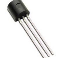
... Drivers (relays, hammers, solenoids, lamps, memories, displays, bipolar transistors, etc.) Ordering Information Package Options Device TO-92 TO-243AA (SOT-89) VP3203 VP3203N3-G -G indicates package is RoHS compliant (‘Green’) * Mil visual screening available. Absolute Maximum Ratings Parameter Drain-to-source voltage Drain-to-gate voltage Gate-to-source voltage Operating and storage temperature ...

Page 2

... V = -25V 1.0MHz -25V -2.0A 10Ω GEN - 300 - 0V PULSE R GEN D.U.T. Output INPUT ● Tel: 408-222-8888 ● www.supertex.com VP3203 I I † DR DRM (mA) (A) -650 -4.0 -1100 -4.0 = -10mA D = -10mA D = -10mA Max Rating DS = 125° -5. -1. -750mA D = -3. -1. -1. -2. -1. -1.0A SD ...

Page 3

... V (volts) DS Power Dissipation vs. Ambient Temperature 2.0 TO-243AA 1.6 1.2 TO-92 0.8 0 100 125 T (°C) A Thermal Response Characteristics 1.0 0.8 TO-243AA 0 25° 1.6W D 0.4 0.2 TO- 25° 0.001 0.01 0.1 1.0 t (seconds) p ● Tel: 408-222-8888 ● www.supertex.com VP3203 -10 150 10 ...

Page 4

... GS 1 -10V GS 0.8 0 -12 -16 I (amperes and R Variation with Temperature (th -10V, -3A DS(ON) 1.2 1.0 0 -10mA (th) 0.6 - 100 T (°C) j Gate Drive Dynamic Characteristics - -10V -20V DS 335pF -4 -2 200 (nanocoulombs) G ● Tel: 408-222-8888 ● www.supertex.com VP3203 -20 1.4 1.2 1.0 0.8 0.6 150 5 ...

Page 5

... Seating Plane E1 1 Symbol A MIN .170 Dimensions NOM - (inches) MAX .210 JEDEC Registration TO-92. * This dimension is not specified in the JEDEC drawing. † This dimension differs from the JEDEC drawing. Drawings not to scale. Supertex Doc.#: DSPD-3TO92N3, Version E041009 Front View Bottom View ...

Page 6

... Supertex inc. does not recommend the use of its products in life support applications, and will not knowingly sell them for use in such applications unless it receives an adequate “product liability indemnification insurance agreement.” Supertex inc. does not assume responsibility for use of devices described, and limits its liability to the replacement of the devices determined defective due to workmanship ...

Related keywords