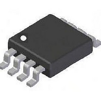
DMN4034SSS-13 Diodes Inc, DMN4034SSS-13 Datasheet - Page 4

DMN4034SSS-13
Manufacturer Part Number
DMN4034SSS-13
Description
MOSFET Small Signal MOSFET,N-CHANNEL 40V, 5.5A/- 7.2A
Manufacturer
Diodes Inc
Datasheet
1.DMN4034SSS-13.pdf
(8 pages)
Specifications of DMN4034SSS-13
Minimum Operating Temperature
- 55 C
Configuration
Dual
Transistor Polarity
N-Channel
Resistance Drain-source Rds (on)
0.023 Ohms
Gate Charge Qg
4.9 nC
Forward Transconductance Gfs (max / Min)
20.5 S
Drain-source Breakdown Voltage
40 V
Gate-source Breakdown Voltage
20 V
Continuous Drain Current
5.4 A
Power Dissipation
1.56 W
Maximum Operating Temperature
+ 150 C
Mounting Style
SMD/SMT
Package / Case
SOIC-8
Lead Free Status / RoHS Status
Lead free / RoHS Compliant
Lead Free Status / RoHS Status
Lead free / RoHS Compliant
Available stocks
Company
Part Number
Manufacturer
Quantity
Price
Company:
Part Number:
DMN4034SSS-13
Manufacturer:
M/A-COM
Quantity:
4 600
Part Number:
DMN4034SSS-13
Manufacturer:
DIODES/美台
Quantity:
20 000
Part Number:
DMN4034SSS-13-F
Manufacturer:
DIODES/美台
Quantity:
20 000
Electrical Characteristics
OFF CHARACTERISTICS
Drain-Source Breakdown Voltage
Zero Gate Voltage Drain Current
Gate-Source Leakage
ON CHARACTERISTICS
Gate Threshold Voltage
Static Drain-Source On-Resistance (Note 7)
Forward Transconductance (Notes 7 & 8)
Diode Forward Voltage (Note 7)
Reverse recovery time (Note 8)
Reverse recovery charge (Note 8)
DYNAMIC CHARACTERISTICS (Note 8)
Input Capacitance
Output Capacitance
Reverse Transfer Capacitance
Total Gate Charge (Note 9)
Total Gate Charge (Note 9)
Gate-Source Charge (Note 9)
Gate-Drain Charge (Note 9)
Turn-On Delay Time (Note 9)
Turn-On Rise Time (Note 9)
Turn-Off Delay Time (Note 9)
Turn-Off Fall Time (Note 9)
Notes:
DMN4034SSS
Document Number DS32106 Rev 1 - 2
7. Measured under pulsed conditions. Pulse width ≤ 300μs; duty cycle ≤ 2%
8. For design aid only, not subject to production testing.
9. Switching characteristics are independent of operating junction temperatures.
Characteristic
@T
A
= 25°C unless otherwise specified
Symbol
R
BV
V
DS (ON)
t
t
I
I
C
V
C
C
GS(th)
Q
Q
D(on)
D(off)
DSS
GSS
Q
Q
Q
g
t
oss
t
t
SD
rss
DSS
rr
iss
fs
gs
gd
r
f
rr
g
g
www.diodes.com
Min
4 of 8
1.0
40
⎯
⎯
⎯
⎯
⎯
⎯
⎯
⎯
⎯
⎯
⎯
⎯
⎯
⎯
⎯
⎯
⎯
0.023
0.039
20.5
0.87
11.9
79.1
40.5
Typ
453
4.9
4.9
1.8
2.4
2.7
2.7
10
14
⎯
⎯
⎯
⎯
6
0.034
0.059
±100
Max
0.5
3.0
1.1
⎯
⎯
⎯
⎯
⎯
⎯
⎯
⎯
⎯
⎯
⎯
⎯
⎯
⎯
⎯
Diodes Incorporated
A Product Line of
Unit
μA
nA
nC
nC
nC
nC
nC
ns
pF
pF
pF
ns
ns
ns
ns
Ω
V
V
S
V
I
V
V
I
V
V
V
I
I
V
f= 1MHz
V
V
V
I
D
D
S
S
D
DS
GS
GS
GS
DS
DS
GS
GS
DD
= 250μA, V
= 6A, V
= 2.5A, di/dt= 100A/μs
= 1A, R
= 250μA, V
= 40V, V
= 15V, I
= 20V, V
= 20V, V
= ±20V, V
= 10V, I
= 4.5V, I
= 4.5V
= 10V
Test Condition
GS
G
DMN4034SSS
≅ 6.0Ω
D
= 0V
D
D
GS
GS
GS
= 6A
= 6A
DS
GS
= 5A
DS
= 0V
= 0V
= 10V
= V
= 0V
= 0V
V
I
© Diodes Incorporated
D
GS
DS
= 6A
= 20V
March 2010


