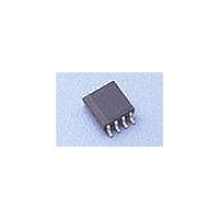
IES5515D Hendon Semiconductors, IES5515D Datasheet - Page 2

IES5515D
Manufacturer Part Number
IES5515D
Description
Buffers & Line Drivers 2.7-5.5V Simple 2 Wire Buffer
Manufacturer
Hendon Semiconductors
Datasheet
1.IES5515T.pdf
(5 pages)
Specifications of IES5515D
Logic Family
IE5515
Supply Voltage (max)
5.5 V
Supply Voltage (min)
2.7 V
Maximum Operating Temperature
85 C
Mounting Style
SMD/SMT
Minimum Operating Temperature
- 40 C
Supply Current
30 mA
Logic Type
Simple 2 Wire Bus Buffer
Package / Case
MSOP-8L
Lead Free Status / RoHS Status
Lead free / RoHS Compliant
5
5.1
6
6.1
The power supply voltage for the IES5505/15 may be any
voltage in the range 2.7 V to 5.5 V. The IC supply must be
common with the supply for the bus. Hysteresis on the
ports is a percentage of the IC’s power supply, hence
noise margin considerations should be taken into account
when selecting an operating voltage.
6.2
The clock signal buffer is uni-directional, though the
direction may be reversed under control of the Direction
pin. In normal bus operations, for example the I
Master device generates a uni-directional clock signal to
the slave. For lowest cost the IES5505/15 combines
uni-directional buffering of the clock signal with a
bi-directional buffer for the data signal. Clock stretching is
therefore not supported and Slave devices that may
require clock stretching must be accommodated by the
Master adopting an appropriate clocking when
communicating with them.The buffer includes hysteresis
to ensure clean switching signals are output, especially
with slow rise times on high capacitively loaded buses.
6.3
The data signal buffer is bi-directional. The port (SDA
SDA
will take control of the buffer direction and “lock out”
signals coming from the opposite side. As the “input” signal
continues to fall, it will then drive the “output” side low.
Again, hysteresis is applied to the buffer to minimise the
effects of noise.
2008 Feb 26, Revision 0.7
PINNING INFORMATION
FUNCTIONAL DESCRIPTION
OUT
SCL
Pinning layout
V
SCL
SDA
SCL
GND
) which first falls below the “lock-out voltage” V
DD
Fig.2 Pinning diagram (SO8 / MSOP8)
OUT
EN
, GND - DC supply pins
IN
IN
IN
, SCL
, SDA
1
2
3
4
OUT
OUT
- Clock Signal inputs/outputs
- Data Signal inputs/outputs
IES5505
IES5515
8
7
6
5
pin5505-8
V
SDA
SDA
DIR
CC
2
C bus, the
OUT
IN
IN
LK
,
,
2
5.2
At some points during the communication, the data
direction will reverse - for example, when the Slave
transmits an acknowledge (ACK), or responds with it’s
register contents. During these times, the controlling
“input” side will have to rise back above the lock-out
voltage (V
allows the “output” side to gain control, and pull (what was)
the “input” side low again. This will cause a “pulse” on the
“input” side, which can be quite large in high capacitance
buses. However, this pulse will not interfere with the actual
data transmission, as it should not occur during times of
clock line transition (during normal I
protocols), and thus data signal set-up time requirements
are still met.
6.4
The active-high Enable input can be used to disable the
buffer, for the purpose of isolating sections of the bus. The
IC should only be disabled when the bus is idle. This
prevents truncation of commands which may confuse
other devices on the bus. Enable may also be used to
progressively activate sections of the bus during system
start-up. Bus sections slow to respond on power-up can be
kept isolated from the main system to avoid interference
and collisions.
6.5
The Direction input is used to change the signal direction
of the SCL ports. When the Direction pin is logic “low”, the
clock signal input is SCL
SCL
signal input is SCL
EN
SCL
SCL
GND
DIR
SDA
SDA
V
SYMBOL
DD
OUT
OUT
IN
IN
OUT
Pin description
Enable (EN) - Activate Buffer Operations
Direction (DIR) - Clock Buffer Direction Control
. When the Direction pin is logic “high”, the clock
LK
IES5505
) before it releases the “lock”, which then
1
2
3
4
5
6
7
8
Simple 2-Wire Bus Buffer
PIN
OUT
and the buffered output is SCL
IN
Enable
Clock Buffer “Slave Side”
Clock Buffer “Master Side”
Supply Ground
Clock Direction
Data Buffer “Master Side”
Data Buffer “Slave Side”
Positive supply
and the buffered output is
Preliminary Specification
DESCRIPTION
IES5515
2
C and SMBus
IN
.


