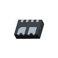
FXMA2102UMX Fairchild Semiconductor, FXMA2102UMX Datasheet - Page 6

FXMA2102UMX
Manufacturer Part Number
FXMA2102UMX
Description
I/O Expanders, Repeaters & Hubs 2xSupply 2-Bit Volt Trnsltr/Bffr/Rptr
Manufacturer
Fairchild Semiconductor
Datasheet
1.FXMA2102UMX.pdf
(16 pages)
Specifications of FXMA2102UMX
Operating Supply Voltage
1.65 V to 5.5 V
Power Dissipation
0.129 mW
Operating Temperature Range
- 40 C to + 85 C
Input Voltage
1.65 V to 5.5 V
Output Current
+/- 50 mA
Output Voltage
- 0.5 V to + 7 V
Package / Case
Ultrathin MLP-8
Lead Free Status / RoHS Status
Lead free / RoHS Compliant
Available stocks
Company
Part Number
Manufacturer
Quantity
Price
Part Number:
FXMA2102UMX
Manufacturer:
FAIRCHILD/ن»™ç«¥
Quantity:
20 000
© 2010 Fairchild Semiconductor Corporation
FXMA2102 • Rev. 1.0.2
Application Notes
The FXMA2102 has open-drain I/Os and requires
external pull-up resistors on the four data I/O pins, as
shown in Figure 4. If a pair of data I/O pins (A
used, both pins should be tied to GND (or both to V
In this case, pull-down or pull-up resistors are not
required. The recommended values for the pull-up
resistors (RPU) are 1KΩ to 10KΩ; however, depending
on the total bus capacitance, the user is free to vary the
pull-up resistor value to meet the maximum I
rate per the I
19, 2007). For example, the maximum edge rate (30% -
70%) during fast mode (400kbit/s) is 300ns. If bus
capacitance is approaching the maximum 400pF, lower
the RPU value to keep the rise time below 300ns (Fast
Mode). Section 7.1 of the I
excellent guideline for pull-up resistor sizing.
Theory of Operation
The FXMA2102 is designed for high-performance level
shifting and buffer / repeating in an I
Figure 1 shows that each bi-directional channel
contains two series-Npassgates and two dynamic
drivers. This hybrid architecture is highly beneficial in an
I
For example, during the following three I
events:
the bus direction needs to change from master to slave
to slave to master without the occurrence of an edge. If
there is an I
in these examples, the I
direction when both A and B ports are LOW. The
Npassgates can accomplish this task very efficiently
because, when both A and B ports are LOW, the
Npassgates act as a low resistive short between the two
(A and B) ports.
Due to I
slaves are not push/pull drivers. Logic LOWs are
“pulled down” (I
state). For example, when the master lets go of SCL
(SCL always comes from the master), the rise time of
SCL is largely determined by the RC time constant,
where R = R
FXMA2102 is attached to the master [on the A port] in
this example, and there is a slave on the B port, the
Npassgates act as a low resistive short between both
2
C application where auto-direction is a necessity.
Clock Stretching
Slave’s ACK Bit (9
Write Bit (8
Clock Synchronization and Multi Master
Arbitration
2
C’s open-drain topology, I
2
C translator between the master and slave
2
PU
C specification (UM10204 rev. 03, June
sink
and C = the bus capacitance. If the
th
), while logic HIGHs are “let go” (3-
bit = 0)
th
bit = 0) following a Master’s
2
2
C translator must change
C specification provides an
2
C masters and
2
C application.
2
C protocol
n
/B
2
n
C edge
) is not
CC
).
6
ports until either of the port’s V
reached. After the RC time constant has reached the
V
triggers both dynamic drivers to drive their respective
ports in the LOW-to-HIGH (LH) direction, accelerating
the rising edge. The resulting rise time resembles the
scope shot in Figure 5. Effectively, two distinct slew
rates appear in rise time. The first slew rate (slower) is
the RC time constant of the bus. The second slew rate
(much faster) is the dynamic driver accelerating the
edge.
If both the A and B ports of the translator are HIGH, a
high-impedance path exists between the A and B ports
because both the Npassgates are turned off. If a master
or slave device decides to pull SCL or SDA LOW, that
device’s driver pulls down (I
edge reaches the A or B port V
either the A or B port threshold is reached, the port’s
edge detector triggers both dynamic drivers to drive
their respective ports in the HIGH-to-LOW (HL)
direction, accelerating the falling edge.
Figure 5. FXMA2102 Waveform C: 600pF, R
CC
/2 threshold of either port, the port’s edge detector
sink
) SCL or SDA until the
CC
CC
/2 threshold. When
/2 thresholds are
www.fairchildsemi.com
PU
: 2.2K


