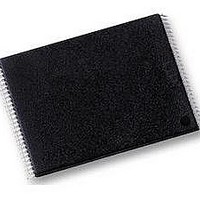
S29GL032N90TFI030 Spansion Inc., S29GL032N90TFI030 Datasheet - Page 45

S29GL032N90TFI030
Manufacturer Part Number
S29GL032N90TFI030
Description
Flash 3V 32Mb Float Gate two address 90s
Manufacturer
Spansion Inc.
Datasheet
1.S29GL032N90TFI010.pdf
(81 pages)
Specifications of S29GL032N90TFI030
Memory Type
NOR
Memory Size
32 Mbit
Access Time
90 ns
Data Bus Width
8 bit, 16 bit
Architecture
Uniform / Boot Sector
Interface Type
Page-mode
Supply Voltage (max)
3.6 V
Supply Voltage (min)
2.7 V
Maximum Operating Current
50 mA
Mounting Style
SMD/SMT
Operating Temperature
+ 85 C
Package / Case
TSOP-48
Ic Interface Type
CFI, Parallel
Supply Voltage Range
2.7V To 3.6V
Memory Case Style
TSOP
No. Of Pins
48
Lead Free Status / RoHS Status
Lead free / RoHS Compliant
Lead Free Status / RoHS Status
Lead free / RoHS Compliant, Lead free / RoHS Compliant
Available stocks
Company
Part Number
Manufacturer
Quantity
Price
Company:
Part Number:
S29GL032N90TFI030
Manufacturer:
SPANSION
Quantity:
6 035
Part Number:
S29GL032N90TFI030
Manufacturer:
SPANSION
Quantity:
20 000
Company:
Part Number:
S29GL032N90TFI030H
Manufacturer:
Spansion
Quantity:
1 440
Part Number:
S29GL032N90TFI030H
Manufacturer:
SPANSION
Quantity:
20 000
October 29, 2008 S29GL-N_01_12
Notes
1. When Sector Address is specified, any address in the selected sector is acceptable. However, when loading Write-Buffer address
2. DQ7 may change simultaneously with DQ5. Therefore, DQ7 should be verified.
3. If this flowchart location was reached because DQ5= 1, then the device FAILED. If this flowchart location was reached because DQ1= 1,
4. See
locations with data, all addresses must fall within the selected Write-Buffer Page.
then the Write to Buffer operation was ABORTED. In either case, the proper reset command must be written before the device can begin
another operation. If DQ1= 1, write the Write-Buffer-Programming-Abort-Reset command. if DQ5= 1, write the Reset command.
Table 10.1 on page 51
DQ1 = 1?
and
D a t a
No
Yes
(Note 1)
Table 10.3 on page 53
(Note 3)
Figure 10.1 Write Buffer Programming Operation
(Note 2)
S29GL-N MirrorBit
Yes
S h e e t
No
Write next address/data pair
Write number of addresses
to program minus 1(WC)
Write first address/data
Write program buffer to
address = Last Loaded
Read DQ7 - DQ0 with
Write “Write to Buffer”
Last Loaded Address
flash sector address
and Sector Address
Read DQ7 - DQ0 at
Buffer Operation?
Sector Address
FAIL or ABORT
command and
WC = WC - 1
Abort Write to
DQ7 = Data?
DQ7 = Data?
DQ5 = 1?
Address
WC = 0 ?
for command sequences required for write buffer programming.
®
Flash Family
Yes
No
No
No
No
Yes
Yes
Yes
Part of “Write to Buffer”
Command Sequence
Write to buffer ABORTED.
Must write “Write-to-buffer
Abort Reset” command
Write to a different
sequence to return
sector address
to read mode.
PASS
45


