MD1813K6-G Supertex, MD1813K6-G Datasheet

MOSFET & Power Driver ICs High Speed Quad

MD1813K6-G

Manufacturer Part Number
MD1813K6-G
Description
MOSFET & Power Driver ICs High Speed Quad
Manufacturer
Supertex
Type
High Side/Low Sider
Datasheet

Specifications of MD1813K6-G

Rise Time
6 ns
Fall Time
6 ns
Supply Voltage (min)
4.5 V
Supply Current
7 mA
Maximum Power Dissipation
2200 mW
Maximum Operating Temperature
+ 85 C
Mounting Style
SMD/SMT
Minimum Operating Temperature
- 20 C
Number Of Drivers
4
Number Of Outputs
4
Package / Case
QFN-16
Lead Free Status / RoHS Status
Lead free / RoHS Compliant

Available stocks

Company
Part Number
Manufacturer
Quantity
Price
Part Number:
MD1813K6-G
Manufacturer:
Supertex
Quantity:
1 837
Features
Applications
Supertex inc.
Typical Application Circuit
6ns rise and fall time
2.0A peak output source/sink current
1.8 to 5.0V input CMOS compatible
Smart Logic threshold
Low jitter design
Quad matched channels
Drives two N and two P-channel MOSFETs
Outputs can swing below ground
Built-in level translator for negative gate bias
Non-inverting gate driver OUTD for easy logic
Low inductance quad flat no-lead package
Thermally-enhanced package
Ultrasound PN code transmitter
Medical ultrasound imaging
Piezoelectric transducer drivers
Nondestructive evaluation
High speed level translator
High voltage bipolar pulser
Logic Inputs
3.3V CMOS
Supertex inc.
PULSE
DAMP
ENAB
High Speed Quad MOSFET Driver
0.22μF
16
15
1
5
6
OE
INA
INB
IND
INC
+10V
GND
3
1235 Bordeaux Drive, Sunnyvale, CA 94089
VDD
14
7
VSS
Supertex
MD1813
2
VL
LT
General Description
The Supertex MD1813 is a high-speed quad MOSFET driver. It is
designed to drive two N- and two P-channel, high voltage, DMOS
FETs for medical ultrasound applications, but may be used in any
application that needs a high output current for a capacitive load.
The input stage of the MD1813 is a high-speed level translator that is
able to operate from logic input signals of 1.8 to 5.0V amplitude. An
adaptive threshold circuit is used to set the level translator threshold to
the average of the input logic 0 and logic 1 levels. The level translator
uses a proprietary circuit, which provides DC coupling together with
high-speed operation.
The output stage of the MD1813 has separate power connections,
enabling the output signal L and H levels to be chosen independently
from the driver supply voltages. As an example, the input logic levels
may be 0 and 1.8V, the control logic may be powered by +5.0 and -
5.0V, and the output L and H levels may be varied anywhere over the
range of -5.0 to +5.0V. The output stage is capable of peak currents
of up to ±2.0 amps, depending on the supply voltages used and load
capacitance. The OE pin serves a dual purpose. First, its logic H
level is used to compute the threshold voltage level for the channel
input level translators. Secondly, when OE is low, the outputs are
disabled, with the A output high and the B output low. This assists
in properly pre-charging the coupling capacitors that may be used
in series in the gate drive circuit of an external PMOS and NMOS. A
built-in level shifter is for PMOS gate negative bias driving. It enables
the user-defined damping control to generate return-to-zero bipolar
output pulses. The MD1813 has a non-inverting driver OUTD for
easy logic.
VNEG
4
11
0.47μF
VH
OUTG
OUTC
OUTD
OUTA
OUTB
+10V
-8.0V
0.47μF
13
12
10
9
8
2.0k
10nF
10nF
10nF
Tel: 408-222-8888
Supertex
Supertex
TC6320
TC2320
+100V
-100V
www.supertex.com
1.0μF
1.0μF
MD1813

Related parts for MD1813K6-G

MD1813K6-G Summary of contents

Page 1

... IND 6 Supertex inc. General Description The Supertex MD1813 is a high-speed quad MOSFET driver designed to drive two N- and two P-channel, high voltage, DMOS FETs for medical ultrasound applications, but may be used in any application that needs a high output current for a capacitive load. The input stage of the MD1813 is a high-speed level translator that is able to operate from logic input signals of 1 ...

Page 2

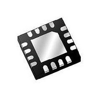
... NEGQ NEG I V average current average current average current NEG NEG Supertex inc. 16-Lead QFN 4.00x4.00mm body 1.00mm height (max) 0.65mm pitch MD1813K6-G Value -0.5V to +13.5V V -0. +0. -0. +0. -7.0V to +0.5V -0.5V to +20V V -10V to V +0. -0.5V to GND +7.0V SS +125°C -65° ...

Page 3

... Output sink resistance for OUTA-D SINK R Output source resistance for OUTA-D SOURCE R Output sink resistance for for OUTG SINK R Output source resistance for OUTG SOURCE I Peak output sink current SINK I Peak output source current SOURCE Supertex inc. (cont.) = -6.0V 3.3V Min Typ V -0 ...

Page 4

... OUTPUT 10 Supertex inc. to prevent resonance in the power supply lead coming to the capacitor. Pay particular attention to minimizing trace lengths, current loop area, and using sufficient trace width to reduce inductance. Surface mount components are highly recommended. Since the output impedance of this driver is ...

Page 5

... OUTA Output driver. 14 VDD Supply voltage for high-side analog, level shifter, and gate drive circuit. 15 INA Logic input. Controls OUTA when OE is high Output enable logic input. Note: Thermal pad and pin #4, VNEG must be connected externally. Supertex inc. INB IND OUTC ● ...

Page 6

... This dimension is not specified in the JEDEC drawing. † This dimension differs from the JEDEC drawing. Drawings not to scale. Supertex Doc.#: DSPD-16QFNK64X4P065, Version C041009. (The package drawing(s) in this data sheet may not reflect the most current specifications. For the latest package outline information go to http://www.supertex.com/packaging.html.) does not recommend the use of its products in life support applications, and will not knowingly sell them for use in such applications unless it receives Supertex inc ...

Related keywords