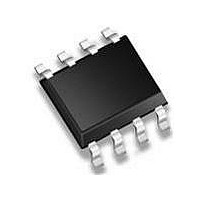
SRK2000D STMicroelectronics, SRK2000D Datasheet - Page 12

SRK2000D
Manufacturer Part Number
SRK2000D
Description
Switching Converters, Regulators & Controllers Synch Rectifier Dual Smart driver LLC
Manufacturer
STMicroelectronics
Series
-r
Datasheet
1.SRK2000D.pdf
(17 pages)
Specifications of SRK2000D
Output Voltage
11.9 V
Output Current
3.5 A
Input Voltage
4.5 V to 32 V
Switching Frequency
500 KHz
Operating Temperature Range
- 40 C to + 150 C
Mounting Style
SMD/SMT
Duty Cycle (max)
60 %
Package / Case
SOIC-8
Number Of Outputs
2
Applications
General Purpose
Voltage - Input
-
Voltage - Supply
4.5 V ~ 32 V
Current - Supply
35mA
Operating Temperature
-40°C ~ 150°C
Mounting Type
*
Lead Free Status / RoHS Status
Lead free / RoHS Compliant
Available stocks
Company
Part Number
Manufacturer
Quantity
Price
Part Number:
SRK2000D
Manufacturer:
ST
Quantity:
20 000
Part Number:
SRK2000DTR
Manufacturer:
ST
Quantity:
20 000
Application information
12/17
higher than twice the output voltage; if this exceeds the voltage rating of the internal clamp
(Vcc
value, lower than the maximum rating (25 mA) and taking the related power dissipation into
account. On the other hand, when current starts flowing into the body diode of one MOSFET
(or in the diode in parallel with the MOSFET), the drain-to-source voltage is negative (
V); when the voltage on pins VDS1-2 reaches the threshold V
internal current source I
MOSFET is turned on. Therefore, the actual triggering threshold can be determined by the
following formula:
For instance, with R
V = -0.3 V.
To avoid false triggering of the gate driver, a debounce delay T
sourcing I
ns before the gate driver is turned on). This delay is not critical for the converter’s efficiency
because the initial current is close to zero or anyway much lower than the peak value.
Once the SR MOSFET has been switched on, its drain-to-source voltage drops to a value
given by the flowing current times the MOSFET R
low, the voltage drop across the R
determine an improper turn-off. To prevent this, the state machine enables the turn-off
comparator referenced to V
on the information of the duration of the previous cycle. In the first half of the conduction
cycle only an additional comparator, referenced to zero, is active to prevent the current of
the SR MOSFET from reversing, which would impair the operation of the LLC converter.
Once the threshold V
the GATE is turned off, the current will again flow through the body diode causing the drain-
to-source voltage to have a negative jump, going again below V
however, prevents a false turn-on.
It is worth pointing out that, due to the fact that each MOSFET is turned on after its body
diode starts conducting, the ON transition happens with the drain-source voltage equal to
the body diode forward drop; therefore there is neither Miller effect nor switching losses at
MOSFET turn-on. Also at turn-off the switching losses are not present, in fact the current is
always flowing from source to drain and, when the MOSFET is switched off, it goes on
flowing through the body diode (or the external diode in parallel to the MOSFET).
Unlike at turn-on, the turn-off speed is critical to avoid current reversal on the secondary
side, especially when the converter operates above the resonance frequency, where the
current flowing through the MOSFET exhibits a very steep edge while decreasing down to
zero: the turn-off propagation T
The interlock logic, in addition to checking for consistent secondary voltage waveforms (one
MOSFET can be turned on only if the other one has a positive drain-to-source voltage >
V
one gate driver has been turned off, it cannot be turned on again before the other gate drive
has had its own on/off cycle.
DVS1,2_A
Z
= 36 V typ.) a series resistor R
DS1,2_On
) to prevent simultaneous conduction, allows only one switching per cycle: after
(i.e. the current sourced by the pin must exceed 50 µA for more than 250
D
DVS1,2_Off
= 2 kΩ, the triggering threshold will be located at -(2 kΩ ⋅ 50 µA) - 0.2
DVS1,2_On
DVS1,2_Off
V
TH
Doc ID 17811 Rev 1
PD_Off
is crossed (in the second half of the conduction cycle) and
−
ON
DS(on)
is activated; as this current exceeds 50 µA, the gate of the
=
D
only in the second half of the conduction cycle, based
delay has a maximum value of 60 ns.
R
has to limit the injected current below an appropriate
D
might exceed the turn-off threshold V
⋅
I
DVS
1
2 ,
On
DS(on)
+
V
DVS
. Again, since the initial current is
1
2 ,
_
TH
DVS1,2_TH
PD_On
TH-ON
(= 250 ns) is used after
. The interlock logic,
(-0.2V typ.) an
DVS1,2_Off
SRK2000
≅
, and
-0.7


