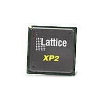
LFXP20C-3FN256C Lattice, LFXP20C-3FN256C Datasheet - Page 36

LFXP20C-3FN256C
Manufacturer Part Number
LFXP20C-3FN256C
Description
FPGA - Field Programmable Gate Array 19.7K LUTS 188 I/O
Manufacturer
Lattice
Specifications of LFXP20C-3FN256C
Number Of Programmable I/os
188
Data Ram Size
405504
Supply Voltage (max)
3.465 V
Maximum Operating Temperature
+ 90 C
Minimum Operating Temperature
0 C
Mounting Style
SMD/SMT
Supply Voltage (min)
1.71 V
Package / Case
FPBGA-256
Lead Free Status / RoHS Status
Lead free / RoHS Compliant
Available stocks
Company
Part Number
Manufacturer
Quantity
Price
Company:
Part Number:
LFXP20C-3FN256C
Manufacturer:
Lattice
Quantity:
135
Company:
Part Number:
LFXP20C-3FN256C
Manufacturer:
Lattice Semiconductor Corporation
Quantity:
10 000
- Current page: 36 of 130
- Download datasheet (2Mb)
Lattice Semiconductor
Initialization Supply Current
I
I
I
1. Until DONE signal is active.
2. For further information on supply current, please see details of additional technical documentation at the end of this data sheet.
3. Assumes all outputs are tristated, all inputs are configured as LVCMOS and held at the V
4. Frequency 0MHz.
5. Typical user pattern.
6. Assume normal bypass capacitor/decoupling capacitor across the supply.
7. T
CC
CCAUX
CCJ
A
=25°C, power supplies at nominal voltage.
Symbol
Core Power Supply
Auxiliary Power Supply
V
V
CCAUX
CCJ
Power Supply
Parameter
= 3.3V
Over Recommended Operating Conditions
1, 2, 3, 4, 5, 6
LFXP10E/C
LFXP20E/C
LFXP15 /C
LFXP3E/C
LFXP6E/C
LFXP10C
LFXP15C
LFXP20C
LFXP10E
LFXP15E
LFXP20E
LFXP3E
LFXP6E
LFXP3C
LFXP6C
Device
3-5
All
DC and Switching Characteristics
CCIO
LatticeXP Family Data Sheet
Typ.
or GND.
110
140
250
150
180
290
110
130
40
50
60
70
50
60
90
2
7
Units
mA
mA
mA
mA
mA
mA
mA
mA
mA
mA
mA
mA
mA
mA
mA
mA
Related parts for LFXP20C-3FN256C
Image
Part Number
Description
Manufacturer
Datasheet
Request
R

Part Number:
Description:
FPGA - Field Programmable Gate Array 19.7K LUTs 340 IO 1. 8/2.5/3.3V -3 Spd I
Manufacturer:
Lattice

Part Number:
Description:
FPGA - Field Programmable Gate Array 19.7K LUTs 268 IO 1. 8/2.5/3.3V -3 Spd
Manufacturer:
Lattice

Part Number:
Description:
FPGA - Field Programmable Gate Array 19.7K LUTs 340 I/O 1.8/2.5/3.3V -3 Spd
Manufacturer:
Lattice
Datasheet:

Part Number:
Description:
FPGA - Field Programmable Gate Array 19.7K LUTs 268 IO 1. 8/2.5/3.3V -3 Spd I
Manufacturer:
Lattice
Part Number:
Description:
FPGA LatticeXP Family 20000 Cells 320MHz 130nm (CMOS) Technology 1.8V/2.5V/3.3V 256-Pin FBGA Tray
Manufacturer:
LATTICE SEMICONDUCTOR
Datasheet:
Part Number:
Description:
FPGA LatticeXP Family 20000 Cells 320MHz 130nm (CMOS) Technology 1.8V/2.5V/3.3V 388-Pin FBGA Tray
Manufacturer:
LATTICE SEMICONDUCTOR
Datasheet:
Part Number:
Description:
FPGA LatticeXP Family 20000 Cells 360MHz 130nm (CMOS) Technology 1.8V/2.5V/3.3V 256-Pin FBGA Tray
Manufacturer:
LATTICE SEMICONDUCTOR
Datasheet:
Part Number:
Description:
FPGA LatticeXP Family 20000 Cells 360MHz 130nm (CMOS) Technology 1.8V/2.5V/3.3V 388-Pin FBGA Tray
Manufacturer:
LATTICE SEMICONDUCTOR
Datasheet:
Part Number:
Description:
FPGA LatticeXP Family 20000 Cells 400MHz 130nm (CMOS) Technology 1.8V/2.5V/3.3V 256-Pin FBGA Tray
Manufacturer:
LATTICE SEMICONDUCTOR
Datasheet:
Part Number:
Description:
FPGA LatticeXP Family 20000 Cells 400MHz 130nm (CMOS) Technology 1.8V/2.5V/3.3V 256-Pin FBGA Tray
Manufacturer:
LATTICE SEMICONDUCTOR
Datasheet:

Part Number:
Description:
IC FPGA 19.7KLUTS 188I/O 256-BGA
Manufacturer:
Lattice
Datasheet:

Part Number:
Description:
IC FPGA 19.7KLUTS 340I/O 484-BGA
Manufacturer:
Lattice
Datasheet:

Part Number:
Description:
IC FPGA 19.7KLUTS 188I/O 256-BGA
Manufacturer:
Lattice
Datasheet:

Part Number:
Description:
IC FPGA 19.7KLUTS 188I/O 256-BGA
Manufacturer:
Lattice
Datasheet:


