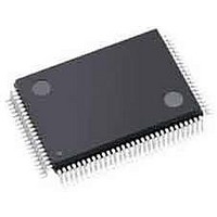
LFXP3C-5TN100C Lattice, LFXP3C-5TN100C Datasheet - Page 206

LFXP3C-5TN100C
Manufacturer Part Number
LFXP3C-5TN100C
Description
FPGA - Field Programmable Gate Array 3.1K LUTS 62 I/O
Manufacturer
Lattice
Specifications of LFXP3C-5TN100C
Number Of Programmable I/os
62
Data Ram Size
55296
Supply Voltage (max)
3.465 V
Maximum Operating Temperature
+ 90 C
Minimum Operating Temperature
0 C
Mounting Style
SMD/SMT
Supply Voltage (min)
1.71 V
Package / Case
TQFP-100
Lead Free Status / RoHS Status
Lead free / RoHS Compliant
Available stocks
Company
Part Number
Manufacturer
Quantity
Price
Company:
Part Number:
LFXP3C-5TN100C
Manufacturer:
Lattice Semiconductor Corporation
Quantity:
10 000
- Current page: 206 of 397
- Download datasheet (10Mb)
Lattice Semiconductor
Figures 9-42 to 9-45 show the behavior of non-pipelined FIFO_DC or FIFO_DC without output registers. When we
pipeline the registers, the output data is delayed by one clock cycle. There is an extra option for output registers to
be enabled by the RdEn signal.
Figures 9-46 to 9-49 show similar waveforms for the FIFO_DC with output register and without output register
enable with RdEn. It should be noted that flags are asserted and de-asserted with similar timing to the FIFO_DC
without output registers. However it is only the data out ‘Q’ that is delayed by one clock cycle.
Figure 9-46. FIFO_DC With Output Registers, Start of Data Write Cycle
RPReset
WrClock
RdClock
Almost
Almost
Empty
Empty
Reset
WrEn
RdEn
Data
Full
Full
Q
Invalid Data
Data_1
Data_2
9-41
Invalid Q
Data_3
LatticeECP/EC and LatticeXP Devices
Data_4
Data_5
Memory Usage Guide
Related parts for LFXP3C-5TN100C
Image
Part Number
Description
Manufacturer
Datasheet
Request
R

Part Number:
Description:
FPGA, 1.8V FLASH, INSTANT ON, SMD
Manufacturer:
LATTICE SEMICONDUCTOR
Datasheet:

Part Number:
Description:
FPGA - Field Programmable Gate Array 3.1K LUTs 100 IO 1.8 /2.5/3.3V -5 Spd
Manufacturer:
Lattice

Part Number:
Description:
FPGA - Field Programmable Gate Array 3.1K LUTs 136 IO 1.8 /2.5/3.3V -5 Spd
Manufacturer:
Lattice

Part Number:
Description:
FPGA - Field Programmable Gate Array 3.1K LUTS 136 I/O
Manufacturer:
Lattice
Datasheet:

Part Number:
Description:
FPGA - Field Programmable Gate Array 3.1K LUTs 100 I/O 1.8/2.5/3.3V -4 Spd
Manufacturer:
Lattice
Datasheet:

Part Number:
Description:
FPGA - Field Programmable Gate Array 3.1K LUTS 62 I/O
Manufacturer:
Lattice
Datasheet:

Part Number:
Description:
FPGA - Field Programmable Gate Array 3.1K LUTs 62 I/O 1.8/2.5/3.3V -4 Spd
Manufacturer:
Lattice
Datasheet:

Part Number:
Description:
FPGA - Field Programmable Gate Array 3.1K LUTs 62 IO 1.8/ 2.5/3.3V -3 Spd I
Manufacturer:
Lattice
Datasheet:

Part Number:
Description:
FPGA - Field Programmable Gate Array 3.1K LUTs 100 I/O 1.8/2.5/3.3V IND
Manufacturer:
Lattice
Datasheet:
Part Number:
Description:
FPGA LatticeXP Family 3000 Cells 320MHz 130nm (CMOS) Technology 1.8V/2.5V/3.3V 208-Pin PQFP Tray
Manufacturer:
LATTICE SEMICONDUCTOR
Datasheet:
Part Number:
Description:
FPGA LatticeXP Family 3000 Cells 320MHz 130nm (CMOS) Technology 1.8V/2.5V/3.3V 144-Pin TQFP Tray
Manufacturer:
LATTICE SEMICONDUCTOR
Datasheet:
Part Number:
Description:
FPGA LatticeXP Family 3000 Cells 360MHz 130nm (CMOS) Technology 1.8V/2.5V/3.3V 100-Pin TQFP Tray
Manufacturer:
LATTICE SEMICONDUCTOR
Datasheet:
Part Number:
Description:
FPGA LatticeXP Family 3000 Cells 360MHz 130nm (CMOS) Technology 1.8V/2.5V/3.3V 144-Pin TQFP Tray
Manufacturer:
LATTICE SEMICONDUCTOR
Datasheet:

Part Number:
Description:
IC FPGA 3.1KLUTS 62I/O 100-TQFP
Manufacturer:
Lattice
Datasheet:


