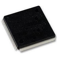
LFXP2-5E-5QN208C Lattice, LFXP2-5E-5QN208C Datasheet - Page 59

LFXP2-5E-5QN208C
Manufacturer Part Number
LFXP2-5E-5QN208C
Description
FPGA - Field Programmable Gate Array 5K LUTs 146I/O Inst- on DSP 1.2V -5 Spd
Manufacturer
Lattice
Datasheet
1.LFXP2-40E-5FN484I.pdf
(92 pages)
Specifications of LFXP2-5E-5QN208C
Number Of Macrocells
5000
Maximum Operating Frequency
200 MHz
Number Of Programmable I/os
146
Data Ram Size
10 KB
Supply Voltage (max)
1.14 V
Supply Current
17 mA
Maximum Operating Temperature
+ 85 C
Minimum Operating Temperature
0 C
Mounting Style
SMD/SMT
Supply Voltage (min)
1.26 V
Package / Case
PQFP-208
Lead Free Status / RoHS Status
Lead free / RoHS Compliant
Available stocks
Company
Part Number
Manufacturer
Quantity
Price
Company:
Part Number:
LFXP2-5E-5QN208C
Manufacturer:
Lattice Semiconductor Corporation
Quantity:
10 000
Part Number:
LFXP2-5E-5QN208C
Manufacturer:
LATTICE
Quantity:
20 000
Lattice Semiconductor
Register-to-Register Performance (Continued)
Derating Timing Tables
Logic timing provided in the following sections of this data sheet and the ispLEVER design tools are worst case
numbers in the operating range. Actual delays at nominal temperature and voltage for best case process, can be
much better than the values given in the tables. The ispLEVER design tool can provide logic timing numbers at a
particular temperature and voltage.
DSP IP Functions
16-Tap Fully-Parallel FIR Filter
1024-pt FFT
8X8 Matrix Multiplication
1. These timing numbers were generated using the ispLEVER design tool. Exact performance may vary with device, design and tool version.
Timing v. A 0.12
The tool uses internal parameters that have been characterized but are not tested on every device.
Function
3-15
DC and Switching Characteristics
LatticeXP2 Family Data Sheet
-7 Timing
198
221
196
Units
MHz
MHz
MHz


