A3P015-QNG68 Actel, A3P015-QNG68 Datasheet - Page 114
A3P015-QNG68
Manufacturer Part Number
A3P015-QNG68
Description
FPGA - Field Programmable Gate Array 15K System Gates
Manufacturer
Actel
Datasheet
1.A3P1000-FGG144.pdf
(218 pages)
Specifications of A3P015-QNG68
Processor Series
A3P015
Core
IP Core
Number Of Macrocells
128
Maximum Operating Frequency
350 MHz
Number Of Programmable I/os
49
Supply Voltage (max)
3.3 V
Supply Current
2 mA
Maximum Operating Temperature
+ 70 C
Minimum Operating Temperature
0 C
Development Tools By Supplier
A3PE-Proto-Kit, A3PE-Brd1500-Skt, Silicon-Explorer II, Silicon-Sculptor 3, SI-EX-TCA, FlashPro 4, FlashPro 3, FlashPro Lite
Mounting Style
SMD/SMT
Supply Voltage (min)
1.5 V
Number Of Gates
15 K
Package / Case
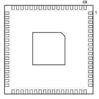
QFN-68
Lead Free Status / RoHS Status
Lead free / RoHS Compliant
Available stocks
Company
Part Number
Manufacturer
Quantity
Price
Company:

Part Number:
A3P015-QNG68
Manufacturer:
ACTEL
Quantity:
954
Company:
Part Number:
A3P015-QNG68PS32
Manufacturer:
VIS
Quantity:
2 722


ProASIC3 DC and Switching Characteristics
Table 2-116 • RAM4K9
2- 10 0
Parameter
t
t
t
t
t
t
t
t
t
t
t
t
t
t
t
t
t
t
t
F
Note:
AS
AH
ENS
ENH
BKS
BKH
DS
DH
CKQ1
CKQ2
C2CWWL
C2CWWH
C2CRWH
C2CWRH
RSTBQ
REMRSTB
RECRSTB
MPWRSTB
CYC
MAX
For specific junction temperature and voltage supply levels, refer to
Commercial-Case Conditions: T
Timing Characteristics
Address setup time
Address hold time
REN_B, WEN_B setup time
REN_B, WEN_B hold time
BLK_B setup time
BLK_B hold time
Input data (DI) setup time
Input data (DI) hold time
Clock High to new data valid on DO (output retained, WMODE = 0)
Clock High to new data valid on DO (flow-through, WMODE = 1)
Clock High to new data valid on DO (pipelined)
Address collision clk-to-clk delay for reliable write after write on same
address—Applicable to Closing Edge
Address collision clk-to-clk delay for reliable write after write on same
address—Applicable to Rising Edge
Address collision clk-to-clk delay for reliable read access after write on same
address—Applicable to Opening Edge
Address collision clk-to-clk delay for reliable write access after read on same
address— Applicable to Opening Edge
RESET_B Low to data out Low on DO (flow-through)
RESET_B Low to Data Out Low on DO (pipelined)
RESET_B removal
RESET_B recovery
RESET_B minimum pulse width
Clock cycle time
Maximum frequency
Description
J
= 70°C, Worst-Case VCC = 1.425 V
R e visio n 9
Table 2-6 on page 2-6
0.25 0.28 0.33
0.00 0.00 0.00
0.14 0.16 0.19
0.10 0.11 0.13
0.23 0.27 0.31
0.02 0.02 0.02
0.18 0.21 0.25
0.00 0.00 0.00
2.36 2.68 3.15
1.79 2.03 2.39
0.89 1.02 1.20
0.33 0.28 0.25
0.30 0.26 0.23
0.45 0.38 0.34
0.49 0.42 0.37
0.92 1.05 1.23
0.92 1.05 1.23
0.29 0.33 0.38
1.50 1.71 2.01
0.21 0.24 0.29
3.23 3.68 4.32
310
–2
for derating values.
272
–1
Std. Units
231
MHz
ns
ns
ns
ns
ns
ns
ns
ns
ns
ns
ns
ns
ns
ns
ns
ns
ns
ns
ns
ns
ns
Related parts for A3P015-QNG68
Image
Part Number
Description
Manufacturer
Datasheet
Request
R

Part Number:
Description:
ProASIC3 Flash Family FPGAs
Manufacturer:
ACTEL [Actel Corporation]
Datasheet:

Part Number:
Description:
MCU, MPU & DSP Development Tools Silicon Sculptor Programming Mod
Manufacturer:
Actel
Part Number:
Description:
MCU, MPU & DSP Development Tools InSystem Programming ProASICPLUS Devices
Manufacturer:
Actel
Part Number:
Description:
Programming Socket Adapters & Emulators PQ160 Module
Manufacturer:
Actel
Part Number:
Description:
Programming Socket Adapters & Emulators Axcelerator Adap Module Kit
Manufacturer:
Actel
Part Number:
Description:
Programming Socket Adapters & Emulators Evaluation
Manufacturer:
Actel
Part Number:
Description:
Programming Socket Adapters & Emulators AFDX Solutions
Manufacturer:
Actel
Part Number:
Description:
Programming Socket Adapters & Emulators SILICON SCULPTOR ADAPTER MODULE
Manufacturer:
Actel
Datasheet:
Part Number:
Description:
Programming Socket Adapters & Emulators Axcelerator Adap Module Kit
Manufacturer:
Actel
Part Number:
Description:
Programming Socket Adapters & Emulators Evaluation
Manufacturer:
Actel
Part Number:
Description:
Programming Socket Adapters & Emulators Silicon Sculptor Software
Manufacturer:
Actel
Part Number:
Description:
Programming Socket Adapters & Emulators InSystem Programming ProASICPLUS Devices
Manufacturer:
Actel
Part Number:
Description:
Programming Socket Adapters & Emulators Evaluation
Manufacturer:
Actel
Part Number:
Description:
Programming Socket Adapters & Emulators Axcelerator Adap Module Kit
Manufacturer:
Actel