DG445DY-E3 Vishay, DG445DY-E3 Datasheet
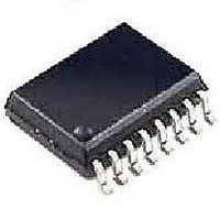
Analog Switch ICs SPST Analog Switch

DG445DY-E3

Manufacturer Part Number
DG445DY-E3
Description
Analog Switch ICs SPST Analog Switch
Manufacturer
Vishay
Datasheets

Specifications of DG445DY-E3

Number Of Switches
Quad
Switch Configuration
SPST
On Resistance (max)
160 Ohms
On Time (max)
450 ns
Off Time (max)
210 ns
Supply Voltage (max)
25 V
Supply Current
0.000001 mA
Maximum Power Dissipation
640 mW
Maximum Operating Temperature
+ 85 C
Mounting Style
SMD/SMT
Package / Case
SOIC-16 Narrow
Minimum Operating Temperature
- 40 C
Analogue Switch Type
SPST
No. Of Channels
4
On State Resistance Max
85ohm
Turn Off Time
160ns
Turn On Time
120ns
Supply Voltage Range
0V To 12V, ± 15V
Operating Temperature Range
-40°C To
Lead Free Status / RoHS Status
Lead free / RoHS Compliant
Lead Free Status / RoHS Status
Lead free / RoHS Compliant, Lead free / RoHS Compliant
The DG444/DG445 monolithic quad analog switches are
designed to provide high speed, low error switching of analog
signals. The DG444 has a normally closed function. The
DG445 has a normally open function. Combining low power
(22 nW, typ)
DG444/DG445 are ideally suited for upgrading DG211/212
sockets. Charge injection has been minimized on the drain for
use in sample-and-hold circuits.
Document Number: 70054
S-52433—Rev. F, 06-Sep-99
Low On-Resistance: 50
Low Leakage: 80 pA
Low Power Consumption: 22 nW
Fast Switching Action—t
Low Charge Injection
DG211/DG212 Upgrades
TTL/CMOS Logic Compatible
GND
IN
IN
D
V–
D
S
S
1
1
1
4
4
4
1
2
3
4
5
6
7
8
with
Dual-In-Line and SOIC
high speed (t
Top View
DG444
ON
Quad SPST CMOS Analog Switches
: 120 ns
ON
: 120 ns, typ), the
16
15
14
13
12
11
10
9
Low Signal Errors and Distortion
Reduced Power Supply
Requirements
Faster Throughput
Improved Reliability
Reduced Pedestal Errors
Simple Interfacing
IN
D
S
V+
V
S
D
IN
2
2
L
3
3
2
3
To achieve high-voltage ratings and superior switching
performance, the DG444/DG445 are built on Vishay Siliconix’s
high-voltage silicon-gate process. An epitaxial layer prevents
latchup.
Each switch conducts equally well in both directions when on,
and blocks input voltages to the supply levels when off.
Temp Range
–40 C to 85 C
–40 C to 85 C
40 C
85 C
Logic
0
1
Audio Switching
Battery Powered Systems
Data Acquisition
Sample-and-Hold Circuits
Telecommunication Systems
Automatic Test Equipment
Single Supply Circuits
Hard Disk Drives
16-Pin Narrow SOIC
16-Pin Narrow SOIC
16-Pin Plastic DIP
16-Pin Plastic DIP
Logic “0”
Logic “1”
Package
www.vishay.com FaxBack 408-970-5600
DG444
OFF
ON
Vishay Siliconix
0.8 V
2.4 V
DG444/445
DG445
Part Number
OFF
ON
DG444DJ
DG445DJ
DG444DY
DG445DY
4-1

Related parts for DG445DY-E3

DG445DY-E3 Summary of contents

Page 1

... Single Supply Circuits Hard Disk Drives Logic DG444 DG445 0 ON OFF 1 OFF ON Logic “0” 0.8 V Logic “1” 2.4 V Package Part Number DG444DJ 16-Pin Plastic DIP 16-Pin Plastic DIP DG445DJ DG444DY 16-Pin Narrow SOIC 16-Pin Narrow SOIC DG445DY www.vishay.com FaxBack 408-970-5600 4-1 ...

Page 2

... Channel On Capacitance C D(on) Power Supplies Positive Supply Current I+ Negative Supply Current I– Logic Supply Current I L Ground Current I GND www.vishay.com FaxBack 408-970-5600 4 Power Dissipation (Package)b c 16-Pin Plastic DIP 25 V 16-Pin Narrow Body SOIC (V–) – (V Notes: a. Signals diodes. Limit forward diode current to maximum current ratings. ...

Page 3

... Room Full Room Full Room Full Room Full DG444/445 Vishay Siliconix D Suffix – Min Typ Max Unit 100 160 200 300 450 200 2 pC 0.001 1 5 –1 –0.0001 – 0.001 1 5 –1 –0.001 –5 www.vishay.com FaxBack 408-970-5600 4-3 ...

Page 4

... Source/Drain Leakage Currents S(off) D(off) 0 –20 I D(on) –40 – V– = –15 V –80 For I (off) –100 –15 –10 – – Drain or Source Voltage ( www.vishay.com FaxBack 408-970-5600 4-4 Crosstak and Off Isolation vs. Frequency –140 –120 –100 –80 –60 –40 –20 0 100 V– –10 – ...

Page 5

... Switching Time vs. Input Voltage 160 V– = –15 V 140 t ON 120 100 OFF 60 DG444 40 DG445 Input Voltage (V) DG444/445 Vishay Siliconix V– DG444 DG445 OFF t OFF – Positive Supply ( V– = – S(on) D(on S(off) D(off) –10 – – Analog Voltage (V) ANALOG 5 www.vishay.com FaxBack 408-970-5600 4-5 ...

Page 6

... V– + V– GND – (includes fixture and stray capacitance + V– GND –15 V www.vishay.com FaxBack 408-970-5600 4-6 Level Shift/ Drive FIGURE Logic Input Switch Input 35 pF Switch 0 V Output Note: Logic input waveform is inverted for DG445. FIGURE 2. Switching Time OFF C (DG444 OFF ...

Page 7

... tantalum in parallel with 0.01 mF ceramic 0V GND V– C –15 V FIGURE 6. Source/Drain Capacitances + DG444 GND V– FIGURE 7. Level Shifter DG444/445 Vishay Siliconix + GND V– C – Off Isolation = 20 log V O FIGURE 5. Off Isolation Meter HP4192A Impedance Analyzer or Equivalent MHz + OUT www.vishay.com FaxBack 408-970-5600 4-7 ...

Page 8

... GAIN GAIN GAIN 100 V DG444 or DG445 V– –15 V FIGURE 8. Precision-Weighted Resistor Programmable-Gain Amplifier +15 V –15 V – 5 www.vishay.com FaxBack 408-970-5600 4-8 + – +15 V Gain error is determined only by the resistor tolerance. Op amp offset and CMRR will limit V+ L accuracy of circuit With OUT GND ...

Related keywords