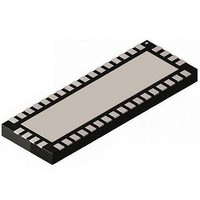
MAX14978ETO+ Maxim Integrated Products, MAX14978ETO+ Datasheet - Page 13

MAX14978ETO+
Manufacturer Part Number
MAX14978ETO+
Description
Analog Switch ICs USB 2.0/3.0 SWITCH High BW LVDS Switch
Manufacturer
Maxim Integrated Products
Datasheet
1.MAX14978ETO.pdf
(15 pages)
Specifications of MAX14978ETO+
On Resistance (max)
10 Ohms
On Time (max)
250 ns
Off Time (max)
50 ns
Off Isolation (typ)
- 17 dB
Bandwidth
950 MHz
Supply Voltage (max)
5.5 V
Supply Voltage (min)
3 V
Supply Current
60 uA
Maximum Power Dissipation
2857 mW
Maximum Operating Temperature
+ 85 C
Mounting Style
SMD/SMT
Package / Case
TQFN-42
Off State Leakage Current (max)
250 nA
Propagation Delay Time
100 ps
Lead Free Status / RoHS Status
Lead free / RoHS Compliant
ESD performance depends on a variety of conditions.
Contact Maxim for a reliability report that documents test
setup, test methodology, and test results.
Figure 6a shows the Human Body Model, and Figure 6b
shows the current waveform it generates when dis-
charged into a low-impedance state. This model consists
of a 100pF capacitor charged to the ESD voltage of inter-
est, which is then discharged into the test device through
a 1.5kI resistor.
The main difference between tests done using the Human
Body Model and IEC 61000-4-2 is higher peak current
in IEC 61000-4-2. Because series resistance is lower in
the IEC 61000-4-2 ESD test model (Figure 7a) the ESD-
withstand voltage measured to this standard is generally
Figure 6a. Human Body ESD Test Model
Figure 6b. Human Body Current Waveform
VOLTAGE
AMPERES
SOURCE
HIGH-
DC
I
P
36.8%
100%
90%
10%
CHARGE-CURRENT-
LIMIT RESISTOR
0
0
1M Ω
R
t
100pF
RL
C
C
S
STORAGE
CAPACITOR
CURRENT WAVEFORM
TIME
RESISTANCE
1500 Ω
DISCHARGE
R
D
t
DL
ESD Test Conditions
Human Body Model
I
R
SuperSpeed USB Passive Switch
PEAK-TO-PEAK RINGING
(NOT DRAWN TO SCALE)
IEC 61000-4-2
DEVICE
UNDER
TEST
(Low/Full/Hi/SuperSpeed)
lower than that measured using the Human Body Model.
Figure 7b shows the current waveform for the Q8kV IEC
61000-4-2 Level 4 ESD Contact Discharge test.
The Air Gap Discharge test involves approaching the
device with a charged probe. The Contact Discharge
method connects the probe to the device before the
probe is energized.
High-speed switches require proper layout and design
procedures for optimum performance. Keep design-
controlled impedance PCB traces as short as pos-
sible or follow impedance layouts per the SuperSpeed
USB specification. Ensure that power-supply bypass
capacitors are placed as close as possible to the device.
Multiple bypass capacitors are recommended. Connect
all grounds and the exposed pad to large ground planes
where possible.
Figure 7a. IEC 61000-4-2 ESD Test Model
Figure 7b. IEC 61000-4-2 ESD Generator Current Waveform
VOLTAGE
SOURCE
t
HIGH-
R
DC
= 0.7ns TO 1ns
CHARGE-CURRENT-
LIMIT RESISTOR
50M Ω TO 100M Ω
100%
90%
10%
I
R
C
150pF
C
S
30ns
STORAGE
CAPACITOR
RESISTANCE
DISCHARGE
330 Ω
R
D
60ns
Layout
DEVICE
UNDER
TEST
t
13


