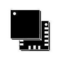
LIS33DE STMicroelectronics, LIS33DE Datasheet - Page 19

LIS33DE
Manufacturer Part Number
LIS33DE
Description
Board Mount Accelerometers MEMS MOTION SENS 3 AXIS 2G/8G SDO NANO
Manufacturer
STMicroelectronics
Datasheet
1.LIS33DE.pdf
(31 pages)
Specifications of LIS33DE
Sensing Axis
Triple
Acceleration
2 g, 8 g
Supply Voltage (max)
3.6 V
Supply Voltage (min)
2.16 V
Supply Current
0.3 mA
Maximum Operating Temperature
+ 85 C
Minimum Operating Temperature
- 40 C
Digital Output - Bus Interface
I2C, SPI
Sensitivity
18 mg/digit, 72 mg/digit
Package / Case
LGA-16
Output Type
Digital
Lead Free Status / RoHS Status
Lead free / RoHS Compliant
Available stocks
Company
Part Number
Manufacturer
Quantity
Price
Company:
Part Number:
LIS33DE
Manufacturer:
STMicroelectronics
Quantity:
1 450
Part Number:
LIS33DE
Manufacturer:
ST
Quantity:
20 000
Company:
Part Number:
LIS33DETR
Manufacturer:
STMicroelectronics
Quantity:
6 400
Part Number:
LIS33DETR
Manufacturer:
ST
Quantity:
20 000
LIS33DE
5.2.1
of CS while the last bit (bit 15, bit 23, ...) starts at the last falling edge of SPC just before the
rising edge of CS.
bit 0: RW bit. When 0, the data DI(7:0) is written into the device. When 1, the data DO(7:0)
from the device is read. In latter case, the chip will drives SDO at the start of bit 8.
bit 1: MS bit. When 0, the address will remains unchanged in multiple read/write
commands. When 1, the address is auto incremented in multiple read/write commands.
bit 2-7: address AD(5:0). This is the address field of the indexed register.
bit 8-15: data DI(7:0) (write mode). This is the data that is written into the device (MSb first).
bit 8-15: data DO(7:0) (read mode). This is the data that is read from the device (MSb first).
In multiple read/write commands further blocks of 8 clock periods are added. When MS bit is
0 the address used to read/write data remains the same for every block. When MS bit is 1
the address used to read/write data is incremented at every block.
The function and the behavior of SDI and SDO remain unchanged.
SPI read
Figure 7.
The SPI read command is performed with 16 clock pulses. Multiple byte read command is
performed adding blocks of 8 clock pulses at the previous one.
bit 0: READ bit. The value is 1.
bit 1: MS bit. When 0 do not increment address, when 1 increment address in multiple
reading.
bit 2-7: address AD(5:0). This is the address field of the indexed register.
bit 8-15: data DO(7:0) (read mode). This is the data that is read from the device (MSb first).
bit 16-... : data DO(...-8). Further data in multiple byte reading.
SDO
SPC
SPI read protocol
SDI
CS
RW
MS
AD5 AD4 AD3 AD2 AD1 AD0
Doc ID 15596 Rev 1
DO7 DO6 DO5 DO4 DO3 DO2 DO1 DO0
Digital interfaces
19/31


