C1812C106M3R2CT500 Kemet, C1812C106M3R2CT500 Datasheet - Page 10
C1812C106M3R2CT500
Manufacturer Part Number
C1812C106M3R2CT500
Description
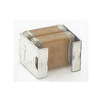
Multilayer Ceramic Capacitors (MLCC) - SMD/SMT 25volts 10uF 20% double chip stack
Manufacturer
Kemet
Datasheet
1.C1812C106M3R2CT500.pdf
(16 pages)
Specifications of C1812C106M3R2CT500
Voltage Rating
25 Volts
Operating Temperature Range
- 55 C to + 125 C
Temperature Coefficient / Code
X7R
Product
Low ESR MLCCs
Dimensions
3.2 mm W x 4.5 mm L x 5 mm H
Termination Style
SMD/SMT
Capacitance
10 uF
Tolerance
20 %
Package / Case
1812 (4532 metric)
Lead Free Status / RoHS Status
Lead free / RoHS Compliant


Surface Mount Multilayer Ceramic Chip Capacitors –KPS Series – Commercial Grade (X7R Dielectric)
Figure 1: Embossed (Plastic) Carrier Tape Dimensions
Table 6 - Embossed (Plastic) Carrier Tape Dimensions
(Metric will govern)
1. The embossment hole location shall be measured from the sprocket hole controlling the location of the embossment. Dimensions of embossment location and
2. The tape with or without components shall pass around R without damage (see Figure 5).
3. If S
4. B1 dimension is a reference dimension for tape feeder clearance only.
5. The cavity defined by A
© KEMET Electronics Corporation • P.O. Box 5928 • Greenville, SC 29606 (864) 963-6300 • www.kemet.com
Tape Size
Tape Size
B
hole location shall be applied independent of each other.
(a) the component does not protrude above the top surface of the carrier tape.
(b) the component can be removed from the cavity in a vertical direction without mechanical restriction, after the top cover tape has been removed.
(c) rotation of the component is limited to 20° maximum for 8 and 12mm tapes and 10° maximum for 16mm tapes (see Figure 3).
(d) lateral movement of the component is restricted to 0.5 mm maximum for 8mm and 12mm wide tape and to 1.0mm maximum for 16mm tape (see Figure 4)
(e) For KPS Series product A
(f) see Addendum in EIA Document 481 for standards relating to more precise taping requirements.
12mm
16mm
12mm
16mm
1
8mm
8mm
S
1
<1.0 mm, there may not be enough area for cover tape to be properly applied (see EIA Document 481 paragraph 4.3 (b)).
1
B
including draft concentric about B
1
is for tape feeder reference only,
T
T
Ko
T
(0.059 +0.004/-0.0)
Cover Tape
2
1
Single (4mm) &
Double (8mm)
1.5 +0.10/-0.0
Triple (12mm)
Single (4mm)
Pitch
D
0
0
, B
Center Lines of Cavity
0
and K
0
and B
o
.
0
shall surround the component with sufficient clearance that:
0
are measured on a plane 0.3mm above the bottom of the pocket.
B
D
(0.039)
(0.059)
(0.323)
(0.476)
Note 1
Note 4
(0.171)
ØDo
1
4.35
1
12.1
8.2
1.0
1.5
User Direction of Unreeling
Max.
Min.
P
Constant Dimensions — Millimeters (Inches)
Variable Dimensions — Millimeters (Inches)
2
(0.069 ± 0.004)
1.75 ± 0.10
Po
P
1
E
(0.246)
(0.404)
(0.561)
10.25
14.25
6.25
2
E
Min.
1
tolerance on tape ±0.2 mm]
[10 pitches cumulative
Ao
ØD
1
(0.157 ± 0.004)
(0.138 ± 0.002)
(0.217 ± 0.002)
(0.217 ± 0.002)
Bo
3.5 ± 0.05
5.5 ± 0.05
5.5 ± 0.05
4.0 ± 0.10
see Note 1 Table 6
Embossment
For cavity size,
P
F
0
F
E
2
E
1
W
(0.079 ± 0.002)
(0.157 ± 0.004)
(0.315 ± 0.004)
(0.315 ± 0.004)
2.0 ± 0.05
4.0 ± 0.10
8.0 ± 0.10
8.0 ± 0.10
P
P
2
1
(0.984)
T
(0.098)
Note 2
(1.181)
(0.181)
(0.181)
R Ref.
25.0
2
2.5
4.6
4.6
30
Max
S
W Max
(0.327)
(0.484)
(0.642)
(0.024)
Note 3
0.600
12.3
16.3
1
8.3
C1020-4 • 6/22/2010
Min.
T Max.
(0.024)
0.600
A
0
Note 5
,B
0
& K
T
(0.004)
0.100
1
Max.
0
10 10
Related parts for C1812C106M3R2CT500
Image
Part Number
Description
Manufacturer
Datasheet
Request
R

Part Number:
Description:
CAP, KEMET #F601BL105K250C
Manufacturer:
Kemet
Datasheet:
Part Number:
Description:
Manufacturer:
Kemet
Datasheet:
Part Number:
Description:
Manufacturer:
Kemet
Datasheet: