ALD555SAL Advanced Linear Devices Inc, ALD555SAL Datasheet
ALD555SAL
Specifications of ALD555SAL
Available stocks


Related parts for ALD555SAL


ALD555SAL Summary of contents
Page 1
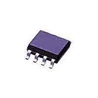
... Small Outline 8-Pin Plastic Package (SOIC) DIP Package ALD555SAL ALD555PAL * Contact factory for leaded (non-RoHS) or high temperature versions. Rev 2.0 ©2010 Advanced Linear Devices, Inc. 415 Tasman Drive, Sunnyvale, CA 94089-1706 Tel: (408) 747-1155 Fax: (408) 747-1286 HIGH SPEED CMOS TIMER ...
Page 2
ABSOLUTE MAXIMUM RATINGS + Supply voltage, V Input voltage range Power dissipation Operating temperature range Storage temperature range Lead temperature, 10 seconds OPERATING ELECTRICAL CHARACTERISTICS +5V unless otherwise specified Parameter Supply ...
Page 3
TYPICAL PERFORMANCE CHARACTERISTICS DISCHARGE OUTPUT SINK CURRENT AS A FUNCTION OF DISCHARGE LOW VOLTAGE 100 + V = 12V 25° 5.0 2.0 1.0 0.5 0.2 0.1 0.01 0.02 0.05 0.1 DISCHARGE LOW VOLTAGE (V) ...
Page 4
TYPICAL PERFORMANCE CHARACTERISTICS (cont'd) OUTPUT SINK CURRENT AS A FUNCTION OF OUTPUT VOLTAGE 100 25° 5.0 2.0 1.0 0.5 0.2 0.1 0.01 0.02 0.05 0.1 OUTPUT VOLTAGE (V) ASTABLE MODE OPERATION 50% DUTY ...
Page 5
S (45° (45° ALD555 SOIC-8 PACKAGE DRAWING 8 Pin Plastic SOIC Package E Dim D ø ø Advanced Linear Devices ...
Page 6
ø ALD555 PDIP-8 PACKAGE DRAWING 8 Pin Plastic DIP Package Dim Min 3. 0. 0.20 c ...
Page 7
ø ALD555 CERDIP-8 PACKAGE DRAWING 8 Pin CERDIP Package Dim D ...