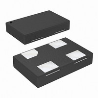
IDT3CP0C02-48NSGE IDT, Integrated Device Technology Inc, IDT3CP0C02-48NSGE Datasheet - Page 5

IDT3CP0C02-48NSGE
Manufacturer Part Number
IDT3CP0C02-48NSGE
Description
IC OSC PROGRAMMABLE TIMER 48MHZ
Manufacturer
IDT, Integrated Device Technology Inc
Type
Programmable Timerr
Specifications of IDT3CP0C02-48NSGE
Current - Supply
2.5mA
Mounting Type
Surface Mount
Frequency
48MHz
Voltage - Supply
1.62 V ~ 3.6 V
Operating Temperature
-20°C ~ 70°C
Package / Case
4-VDFN
Lead Free Status / RoHS Status
Lead free / RoHS Compliant
Count
-
Lead Free Status / Rohs Status
Compliant
3C02 Preliminary Data Sheet
3C02 REVISION B DATE, 10/20/2010
Electrical Characteristics
VDD=1.62V to 1.98V, T
Notes 1. Measured with a 50Ω to GND termination
2: Measured at 48MHz output frequency
3. The 3C02 will support continuous VDD operation from 1.62 to 3.6V. The device can be powered up with a supply voltage at any of the 3 main supply rails of 1.8V, 2.5V or 3.3V.
4. Measured over 1000 cycles per JEDEC standard 65
5. Electrical parameters are guaranteed by design and characterization over the specified ambient operating temperature range, which is established when the device is mounted in a
test socket with maintained transverse airflow greater than 500lfpm. The device will meet specifications after thermal equilibrium has been reached under these conditions.
Application Diagram
Below is a representative application diagram to evaluate the 3C02. For 50Ohm terminated measurements, a balun is necessary to provide
proper impedance matching
ElectroStaticDischa
Frequency Stability
Output HIGH level
Quiescent Current
Output LOW level
Output Frequency
Cycle-cycle Jitter
Input HIGH level
Input LOW level
Supply Voltage
Supply Current
Power-up time
Phase Noise
Period Jitter
Parameter
Duty Cycle
Rise Time
Fall Time
rge
A
=-20 to 70
Symbol
PJ
IDDQ
F
F
ESD
VDD
V
IDD
V
V
DC
PN
o
V
RT
FT
t
CJ
OUT
TOT
OH
on
RMS
C unless otherwise noted. Typical values are measured at VDD=1.8V, T
OL
IH
IL
variation,aging (1st year at 35oC),shock&vibration. “E” device
Factory Programmable.Contact IDT for frequencies not listed
Output valid time after VDD meets the specified range&CE
The absolute value of max change in the periods of any 2
Active supply current, VDD=1.8V, T=35oC, no output load
20% to 80% x VDD. Output load (C
80% to 20% x VDD. Output load (C
Clock output duty cycle. Measured at VDD/2, C
Total Frequency Stability over temperature,supply
Human Body Model, tested per JESD D22-A114
Total RMS Period Jitter (including random and
5
[1.8V]
option, over -20 to 70
1MHz offset from carrier
CE=LOW, output disabled
adjacent cycles
Normal Operation
deterministic)
I
I
Conditions
OH
OL
transition
CE pin
CE pin
= -1.8mA
= 1.8mA
1,2
1,2,4
o
C range
L
L
3
) =4pF, NSG-option
) =4pF, NSG-option
5
1,2
L
=4pF
A
=35
o
C
VDD*0.7
VDD-0.3
4000
1.62
Min
-0.3
45
50
12,48,75,125
©2010 Integrated Device Technology, Inc.
-140
Typ
100
1.8
2.0
0.2
3.5
VDD+0.3
VDD*0.3
+100
-135
Max
1.98
2.75
2.75
400
2.5
0.3
55
50
1
CMOS OSCILLATOR
dBc/Hz
ps
Units
MHz
ppm
mA
µA
ns
ns
µs
ps
%
V
V
V
V
V
V
RMS


