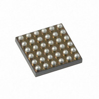
AS1119-BWLT austriamicrosystems, AS1119-BWLT Datasheet - Page 10

AS1119-BWLT
Manufacturer Part Number
AS1119-BWLT
Description
IC LED 144CH DRIVER 36WLCSP
Manufacturer
austriamicrosystems
Datasheet
1.AS1119-BWLT.pdf
(31 pages)
Specifications of AS1119-BWLT
Display Type
LED
Configuration
Dot Matrix
Interface
I²C
Current - Supply
4mA
Voltage - Supply
2.7 V ~ 5.5 V
Operating Temperature
-40°C ~ 85°C
Mounting Type
Surface Mount
Package / Case
36-UFBGA, 36-WLCSP
Lead Free Status / RoHS Status
Lead free / RoHS Compliant
Digits Or Characters
-
Other names
AS1119-BWLTTR
Available stocks
Company
Part Number
Manufacturer
Quantity
Price
Company:
Part Number:
AS1119-BWLT
Manufacturer:
MITSUBISHI
Quantity:
76
Part Number:
AS1119-BWLT
Manufacturer:
AMS
Quantity:
20 000
AS1119
Datasheet - D e t a i l e d D e s c r i p t i o n
I²C Interface
The AS1119 supports the I²C serial bus and data transmission protocol in fast mode at 1MHz. The AS1119 operates as
a slave on the I²C bus. The bus must be controlled by a master device that generates the serial clock (SCL), controls
the bus access, and generates the START and STOP conditions. Connections to the bus are made via the open-drain
I/O pins SCL and SDA.
Figure 14. I²C Interface Initialisation
Figure 15. Bus Protocol
The bus protocol (as shown in
The bus conditions are defined as:
www.austriamicrosystems.com/LED-Driver-ICs/AS1119
- Data transfer may be initiated only when the bus is not busy.
- During data transfer, the data line must remain stable whenever the clock line is HIGH. Changes in the data line
- Bus Not Busy. Data and clock lines remain HIGH.
- Start Data Transfer. A change in the state of the data line, from HIGH to LOW, while the clock is HIGH, defines a
- Stop Data Transfer. A change in the state of the data line, from LOW to HIGH, while the clock line is HIGH,
- Data Valid. The state of the data line represents valid data, when, after a START condition, the data line is stable
- Acknowledge: Each receiving device, when addressed, is obliged to generate an acknowledge after the recep-
SDA
SDI
SCL
SCL
while the clock line is HIGH will be interpreted as control signals.
START condition.
defines the STOP condition.
for the duration of the HIGH period of the clock signal. There is one clock pulse per bit of data.
Each data transfer is initiated with a START condition and terminated with a STOP condition. The number of data
bytes transferred between START and STOP conditions is not limited and is determined by the master device.
The information is transferred byte-wise and each receiver acknowledges with a ninth-bit.
Within the I²C bus specifications a high-speed mode (3.4MHz clock rate) is defined.
tion of each byte. The master device must generate an extra clock pulse that is associated with this acknowledge
bit. A device that acknowledges must pull down the SDA line during the acknowledge clock pulse in such a way
that the SDA line is stable LOW during the HIGH period of the acknowledge clock pulse. Of course, setup and
hold times must be taken into account. A master must signal an end of data to the slave by not generating an
START
A0 and A1 are defined by the pins AD0 and AD1. Pin AD0 and AD1 must not be left floating.
0
1
1
MSB
1
1
Slave Address
1
Figure
2
0
Direction Bit
15) is defined as:
A1
R/W
A0 R/W
6
8
7
9
Revision 1.03
8
D15 D14 D13 D12 D11 D10 D9
1
ACK
9
ACK from
Receiver
1
Repeat if More Bytes Transferred
2
ACK from
Receiver
3-8
8
D8
8
ACK
9
9
Repeated
STOP or
START
10 - 31


