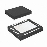
LP3906SQ-TKXII/NOPB National Semiconductor, LP3906SQ-TKXII/NOPB Datasheet - Page 34

LP3906SQ-TKXII/NOPB
Manufacturer Part Number
LP3906SQ-TKXII/NOPB
Description
IC REG BUCK/LDO DUAL 1.5A 300MA
Manufacturer
National Semiconductor
Series
PowerWise®r
Datasheet
1.LP3906SQ-DJXINOPB.pdf
(40 pages)
Specifications of LP3906SQ-TKXII/NOPB
Applications
Digital Cores
Current - Supply
60µA
Voltage - Supply
2.7 V ~ 5.5 V
Operating Temperature
-40°C ~ 85°C
Mounting Type
Surface Mount
Package / Case
24-WFQFN Exposed Pad
Lead Free Status / RoHS Status
Lead free / RoHS Compliant
www.national.com
Note that the output voltage ripple is dependent on the induc-
tor current ripple and the equivalent series resistance of the
output capacitor (R
well as temperature dependent. The R
lated with the applicable switching frequency and ambient
temperature.
I
Both I
resistors connected to VINLDO12 or to the power supply of
the I
∼
C
C
C
C
2
Capacitor
C Pullup Resistor
1.8kΩ) are determined by the capacitance of the bus. Too
LDO1
LDO2
SW1
SW2
2
C master. The values of the pull-up resistors (typ.
2
C_SDA and I
Value
0.47
0.47
10.0
10.0
Min
ESR
2
Unit
C_SCL terminals need to have pullup
). The R
µF
µF
µF
µF
LDO1 output
capacitor
LDO2 output
capacitor
SW1 output
capacitor
SW2 output
capacitor
Description
ESR
is frequency dependent as
ESR
Ceramic, 6.3V,
X5R
Ceramic, 6.3V,
X5R
Ceramic, 6.3V,
X5R
Ceramic, 6.3V,
X5R
Recommended
should be calcu-
Type
34
large of a resistor combined with a given bus capacitance will
result in a rise time that would violate the max. rise time spec-
ification. A too small resistor will result in a contention with the
pull-down transistor on either slave(s) or master.
Operation without I
Operation of the LP3906 without the I
if the system can operate with default values for the LDO and
Buck regulators. (Read below: Factory programmable op-
tions). The I
output values of the LDO and Buck converters.
Factory Programmable Options
The following options are EPROM programmed during final
test of the LP3906. The system designer that needs specific
options is advised to contact the local National Semiconduc-
tor sales office.
The I
The current value equals 0x60.
Factory programmable options
Enable delay for power on
SW1 ramp speed
SW2 ramp speed
2
C Chip ID address is offered as a metal mask option.
2
C-less system must rely on the correct default
2
C Interface
2
C interface is possible
Current value
Control 1 register
code 010 (see
8 mV/µs
8 mV/µs
section)


