EVAL-ADF4360-4EBZ1 Analog Devices Inc, EVAL-ADF4360-4EBZ1 Datasheet - Page 11
EVAL-ADF4360-4EBZ1
Manufacturer Part Number
EVAL-ADF4360-4EBZ1
Description
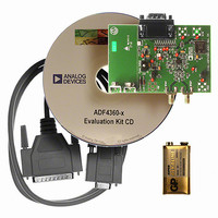
BOARD EVALUATION FOR ADF4360-4
Manufacturer
Analog Devices Inc
Datasheet
1.ADF4360-4BCPZ.pdf
(24 pages)
Specifications of EVAL-ADF4360-4EBZ1
Main Purpose
Timing, Frequency Synthesizer
Embedded
No
Utilized Ic / Part
ADF4360-4
Primary Attributes
Single Integer-N PLL with VCO
Secondary Attributes
1.6GHz, 200kHz PFD
Lead Free Status / RoHS Status
Lead free / RoHS Compliant


The operating current in the VCO core is programmable in four
steps: 5 mA, 10 mA, 15 mA, and 20 mA. This is controlled by
Bits PC1 and PC2 in the control latch.
OUTPUT STAGE
The RF
nected to the collectors of an NPN differential pair driven by
buffered outputs of the VCO, as shown in Figure 15. To allow
the user to optimize the power dissipation versus the output
power requirements, the tail current of the differential pair is
programmable via Bits PL1 and PL2 in the control latch. Four
current levels may be set: 3.5 mA, 5 mA, 7.5 mA, and 11 mA.
These levels give output power levels of −12 dBm, −9 dBm,
−6 dBm, and −3dBm, respectively, using a 50 Ω resistor to V
and ac coupling into a 50 Ω load. Alternatively, both outputs
can be combined in a 1 + 1:1 transformer or a 180° microstrip
coupler (see the Output Matching section).
OUT
A and RF
OUT
B pins of the ADF4360 family are con-
DD
Rev. A | Page 11 of 24
If the outputs are used individually, the optimum output stage
consists of a shunt inductor to V
Another feature of the ADF4360 family is that the supply current
to the RF output stage is shut down until the part achieves lock as
measured by the digital lock detect circuitry. This is enabled by the
mute-till-lock detect (MTLD) bit in the control latch.
VCO
Figure 15. Output Stage ADF4360-4
DIVIDE BY 2
BUFFER/
DD
RF
.
OUT
A
RF
OUT
ADF4360-4
B
Related parts for EVAL-ADF4360-4EBZ1
Image
Part Number
Description
Manufacturer
Datasheet
Request
R

Part Number:
Description:
±1.7g Dual-Axis IMEMS Accelerometer Evaluation Board
Manufacturer:
Analog Devices Inc
Datasheet:

Part Number:
Description:
Inertial Sensor Evaluation System
Manufacturer:
Analog Devices Inc
Datasheet:
Part Number:
Description:
Manufacturer:
Analog Devices Inc
Datasheet:
Part Number:
Description:
Manufacturer:
Analog Devices Inc
Datasheet:
Part Number:
Description:
Manufacturer:
Analog Devices Inc
Datasheet:
Part Number:
Description:
Manufacturer:
Analog Devices Inc
Datasheet:
Part Number:
Description:
Manufacturer:
Analog Devices Inc
Datasheet:
Part Number:
Description:
Manufacturer:
Analog Devices Inc
Datasheet:
Part Number:
Description:
Manufacturer:
Analog Devices Inc
Datasheet:
Part Number:
Description:
Manufacturer:
Analog Devices Inc
Datasheet:
Part Number:
Description:
Manufacturer:
Analog Devices Inc
Datasheet:
Part Number:
Description:
Manufacturer:
Analog Devices Inc
Datasheet:
Part Number:
Description:
Manufacturer:
Analog Devices Inc
Datasheet: