EVAL-ADF4360-8EBZ1 Analog Devices Inc, EVAL-ADF4360-8EBZ1 Datasheet - Page 23
EVAL-ADF4360-8EBZ1
Manufacturer Part Number
EVAL-ADF4360-8EBZ1
Description
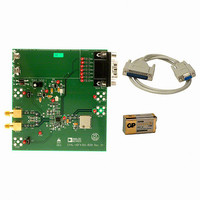
BOARD EVALUATION FOR ADF4360-8
Manufacturer
Analog Devices Inc
Datasheet
1.ADF4360-8BCPZRL7.pdf
(24 pages)
Specifications of EVAL-ADF4360-8EBZ1
Main Purpose
Timing, Frequency Synthesizer
Embedded
No
Utilized Ic / Part
ADF4360-8
Primary Attributes
Single Integer-N PLL with VCO
Secondary Attributes
120MHz, 1MHz PFD
Silicon Manufacturer
Analog Devices
Application Sub Type
Integer-N Synthesizer
Kit Application Type
Clock & Timing
Silicon Core Number
ADF4360-8
Kit Contents
Board
Frequency
400MHz
Rohs Compliant
Yes
Lead Free Status / RoHS Status
Lead free / RoHS Compliant
Other names
Q4990657


OUTPUT MATCHING
There are a number of ways to match the output of the
ADF4360-8 for optimum operation; the most basic is to use a
50 Ω resistor to V
connected in series, as shown in Figure 27. Because the resistor
is not frequency dependent, this provides a good broadband
match. The output power in the circuit below typically gives
−9 dBm output power into a 50 Ω load.
A better solution is to use a shunt inductor (acting as an RF
choke) to V
output power.
Experiments have shown that the circuit shown in Figure 28
provides an excellent match to 50 Ω over the operating range of
the ADF4360-8. This gives approximately 0 dBm output power
across the specific frequency range of the ADF4360-8 using the
recommended shunt inductor, followed by a 100 pF dc blocking
capacitor.
VCO.
Figure 28. Optimum ADF4360-8 Output Stage
Figure 27. Simple ADF4360-8 Output Stage
This gives a better match and, therefore, more
RF
RF
VCO
V
V
VCO
OUT
VCO
OUT
. A dc bypass capacitor of 100 pF is
51Ω
L
100pF
100pF
50Ω
50Ω
Rev. A | Page 23 of 24
The recommended value of this inductor changes with the VCO
center frequency. A graph of the optimum inductor value vs.
frequency is shown in Figure 29.
Both complementary architectures can be examined using the
EVAL-ADF4360-8EB1 evaluation board. If the user does not
need the differential outputs available on the ADF4360-8, the
user should either terminate the unused output or combine
both outputs using a balun. Alternatively, instead of the LC
balun, both outputs may be combined using a 180° rat-race
coupler.
300
250
200
150
100
50
0
0
Figure 29. Optimum ADF4360-8 Shunt Inductor
100
CENTRE FREQUENCY (MHz)
200
300
ADF4360-8
400
5000
Related parts for EVAL-ADF4360-8EBZ1
Image
Part Number
Description
Manufacturer
Datasheet
Request
R

Part Number:
Description:
±1.7g Dual-Axis IMEMS Accelerometer Evaluation Board
Manufacturer:
Analog Devices Inc
Datasheet:

Part Number:
Description:
Inertial Sensor Evaluation System
Manufacturer:
Analog Devices Inc
Datasheet:
Part Number:
Description:
Manufacturer:
Analog Devices Inc
Datasheet:
Part Number:
Description:
Manufacturer:
Analog Devices Inc
Datasheet:
Part Number:
Description:
Manufacturer:
Analog Devices Inc
Datasheet:
Part Number:
Description:
Manufacturer:
Analog Devices Inc
Datasheet:
Part Number:
Description:
Manufacturer:
Analog Devices Inc
Datasheet:
Part Number:
Description:
Manufacturer:
Analog Devices Inc
Datasheet:
Part Number:
Description:
Manufacturer:
Analog Devices Inc
Datasheet:
Part Number:
Description:
Manufacturer:
Analog Devices Inc
Datasheet:
Part Number:
Description:
Manufacturer:
Analog Devices Inc
Datasheet:
Part Number:
Description:
Manufacturer:
Analog Devices Inc
Datasheet:
Part Number:
Description:
Manufacturer:
Analog Devices Inc
Datasheet: