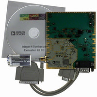
EVAL-ADF411XEBZ1 Analog Devices Inc, EVAL-ADF411XEBZ1 Datasheet - Page 20
EVAL-ADF411XEBZ1
Manufacturer Part Number
EVAL-ADF411XEBZ1
Description
BOARD EVAL FOR ADF411X NO CHIP
Manufacturer
Analog Devices Inc
Datasheet
1.ADF4113BRUZ.pdf
(28 pages)
Specifications of EVAL-ADF411XEBZ1
Main Purpose
Timing, Frequency Synthesizer
Embedded
No
Utilized Ic / Part
ADF4001, ADF4106, ADF4107, ADF4110, ADF4111, ADF4112, ADF4113, ADF4116, ADF4117, ADF4118, ADF4153
Primary Attributes
Single Fractional-N or Integer-N PLL
Secondary Attributes
Board excludes Loop Filter, Synthesizer & VCO
Lead Free Status / RoHS Status
Lead free / RoHS Compliant


ADF4110/ADF4111/ADF4112/ADF4113
Note that there is an enable feature on the timer counter. It is
enabled when Fastlock Mode 2 is chosen by setting the fastlock
mode bit (DB10) in the function latch to 1.
Charge Pump Currents
CPI3, CPI2, and CPI1 program Current Setting 1 for the charge
pump. CPI6, CPI5, and CPI4 program Current Setting 2 for the
charge pump. The truth table is given in Table 10.
Prescaler Value
P2 and P1 in the function latch set the prescaler values. The
prescaler value should be chosen so that the prescaler output
frequency is always less than or equal to 200 MHz. Thus, with
an RF frequency of 2 GHz, a prescaler value of 16/17 is valid but
a value of 8/9 is not.
PD Polarity
This bit sets the phase detector polarity bit. See Table 10.
CP Three-State
This bit controls the CP output pin. With the bit set high, the CP
output is put into three-state. With the bit set low, the CP output
is enabled.
INITIALIZATION LATCH
When C2, C1 = 1, 1, the initialization latch is programmed. This
is essentially the same as the function latch (programmed when
C2, C1 = 1, 0).
However, when the initialization latch is programmed, an addi-
tional internal reset pulse is applied to the R and AB counters.
This pulse ensures that the AB counter is at load point when the
AB counter data is latched, and the device begins counting in
close phase alignment.
If the latch is programmed for synchronous power-down (CE
pin high; PD1 bit high; PD2 bit low), the internal pulse also
triggers this power-down. The prescaler reference and the
oscillator input buffer are unaffected by the internal reset pulse,
so close phase alignment is maintained when counting resumes.
When the first AB counter data is latched after initialization, the
internal reset pulse is again activated. However, successive AB
counter loads after this will not trigger the internal reset pulse.
DEVICE PROGRAMMING AFTER INITIAL
POWER-UP
After initial power-up of the device, there are three ways to
program the device.
Initialization Latch Method
Apply V
input word). Make sure the F1 bit is programmed to 0. Then, do
an R load (00 in 2 LSBs). Then do an AB load (01 in 2 LSBs).
DD
. Program the initialization latch (11 in 2 LSBs of
Rev. C | Page 20 of 28
When the initialization latch is loaded, the following occurs:
1.
2.
3.
CE Pin Method
1.
2.
3.
4.
After CE goes high, a duration of 1 µs may be required for the
prescaler band gap voltage and oscillator input buffer bias to
reach steady state.
CE can be used to power the device up and down in order to
check for channel activity. The input register does not need to
be reprogrammed each time the device is disabled and enabled
as long as it has been programmed at least once after V
initially applied.
Counter Reset Method
1.
2.
3.
This sequence provides the same close alignment as the initiali-
zation method. It offers direct control over the internal reset.
Note that counter reset holds the counters at load point and
three states the charge pump but does not trigger synchronous
power-down. The counter reset method requires an extra
function latch load compared to the initialization latch method.
The function latch contents are loaded.
An internal pulse resets the R, A, B, and timeout counters
to load state conditions and three-states the charge pump.
Note that the prescaler band gap reference and the oscil-
lator input buffer are unaffected by the internal reset pulse,
allowing close phase alignment when counting resumes.
Latching the first AB counter data after the initialization
word activates the same internal reset pulse. Successive AB
loads do not trigger the internal reset pulse unless there is
another initialization.
Apply V
Bring CE low to put the device into power-down. This is an
asynchronous power-down in that it happens immediately.
Program the function latch (10). Program the R counter
latch (00). Program the AB counter latch (01).
Bring CE high to take the device out of power-down. The R
and AB counters now resume counting in close alignment.
Apply V
Do a function latch load (10 in 2 LSBs). As part of this, load
1 to the F1 bit. This enables the counter reset.
Do an R counter load (00 in 2 LSBs). Do an AB counter
load (01 in 2 LSBs). Do a function latch load (10 in 2 LSBs).
As part of this, load 0 to the F1 bit. This disables the
counter reset.
DD
DD
.
.
DD
was
Related parts for EVAL-ADF411XEBZ1
Image
Part Number
Description
Manufacturer
Datasheet
Request
R

Part Number:
Description:
IC, ADJ LDO REG, 1.5V TO 5V 250mA MSOP-8
Manufacturer:
Vishay
Datasheet:

Part Number:
Description:
IC, ADJ LDO REG, 1.5V TO 5V 0.6A 8-TSSOP
Manufacturer:
Vishay
Datasheet:
Part Number:
Description:
IC, ADJ LDO REG, 1.5V TO 5V 250mA MSOP-8
Manufacturer:
Vishay
Datasheet:

Part Number:
Description:
IC ADJ LDO REG 1.5V TO 5V 150mA 5-SOT-23
Manufacturer:
Vishay
Datasheet:

Part Number:
Description:
BOARD EVAL AS1324-AD
Manufacturer:
austriamicrosystems
Datasheet:
Part Number:
Description:
IC, ADJ LDO REG, 1.5V TO 5V 0.6A 8-TSSOP
Manufacturer:
Vishay
Datasheet:

Part Number:
Description:
IC, ADJ LDO REG, 1.5V TO 5V, 0.3A, MSOP8
Manufacturer:
Vishay
Datasheet:
Part Number:
Description:
IC, ADJ LDO REG, 1.5V TO 5V, 0.3A, MSOP8
Manufacturer:
Vishay
Datasheet:
Part Number:
Description:
IC, ADJ LDO REG 1.215V TO 5V 0.3A MSOP-8
Manufacturer:
Vishay
Datasheet:
Part Number:
Description:
IC, ADJ LDO REG 1.215V TO 5V 0.3A MSOP-8
Manufacturer:
Vishay
Datasheet:

Part Number:
Description:
±1.7g Dual-Axis IMEMS Accelerometer Evaluation Board
Manufacturer:
Analog Devices Inc
Datasheet:

Part Number:
Description:
IC MULTIPLIER ANALOG 8-SOIC T/R
Manufacturer:
Analog Devices Inc
Datasheet:

Part Number:
Description:
IC ANALOG MULTIPLIER 8-DIP
Manufacturer:
Analog Devices Inc
Datasheet:
Part Number:
Description:
IC ANALOG MULTIPLIER 8-SOIC
Manufacturer:
Analog Devices Inc
Datasheet:
Part Number:
Description:
IC ANALOG MULTIPLIER 8-DIP
Manufacturer:
Analog Devices Inc
Datasheet: