CP2110EK Silicon Laboratories Inc, CP2110EK Datasheet
CP2110EK
Specifications of CP2110EK
Available stocks


Related parts for CP2110EK


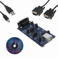
CP2110EK Summary of contents
Page 1
HID USB INGLE H IP Single-Chip HID USB to UART Data Transfer Integrated USB transceiver; no external resistors required Integrated clock; no external crystal required Integrated 343-byte one-time programmable ROM for storing customizable product ...
Page 2
CP2110 2 Rev. 1.0 ...
Page 3
T C ABLE O F ONTENTS Section 1. System Overview . . . . . . . . . . . . . . . . . . . . . . . . . . . . . . ...
Page 4
... MHz to 47 kHz), RS-485 transceiver control, and TX and RX LED toggle. Support for I/O interface voltages down to 1 provided via evaluation kit for the CP2110 (Part Number: CP2110EK) is available. It includes a CP2110-based USB-to- UART/RS-232 evaluation board, Windows DLL and test application, USB and RS-232 cables, and full documentation ...
Page 5
Electrical Characteristics Table 1. Absolute Maximum Ratings Parameter Ambient Temperature under Bias Storage Temperature Voltage on RST, GPIO or UART Pins with respect to GND Voltage with respect to GND DD IO Maximum Total Current ...
Page 6
CP2110 Table 3. UART and Suspend I/O DC Electrical Characteristics V = 1.8 to 3.6 V, –40 to +85 °C unless otherwise specified. IO Parameters Output High Voltage ( Output Low Voltage ( Input High Voltage ...
Page 7
Table 5. Voltage Regulator Electrical Specifications –40 to +85 °C unless otherwise specified. Parameter Input Voltage Range Output Voltage VBUS Detection Input Threshold Bias Current *Note: The maximum regulator supply current is 100 mA. This includes the supply current of ...
Page 8
CP2110 3. Pinout and Package Definitions Name Pin # Type V 6 Power In DD Power Out V 5 Power In I/O Supply Voltage Input. IO GND 2 RST 9 D I/O REGIN 7 Power Regulator Input. ...
Page 9
Table 7. CP2110 Pin Definitions (Continued) Name Pin # Type GPIO.5 18* D I/O RXT D Out GPIO.6 15* D I/O GPIO.7 14* D I/O GPIO.8 13* D I/O GPIO.9 12* D I/O SUSPEND 11* D Out SUSPEND 17* D ...
Page 10
CP2110 GPIO.0_CLK 1 GND VIO 5 VDD 6 Figure 2. QFN-24 Pinout Diagram (Top View) 10 CP2110-GM Top View GND (optional) Rev. 1.0 18 GPIO.5_RXT 17 SUSPEND 16 VPP GPIO GPIO.7 13 GPIO.8 ...
Page 11
QFN-24 Package Specifications Table 8. QFN-24 Package Dimensions Dimension Min A 0.70 A1 0.00 b 0.18 D 4.00 BSC. D2 2.55 e 0.50 BSC. E 4.00 BSC. E2 2.55 Notes: 1. All dimensions shown are in millimeters (mm) unless ...
Page 12
CP2110 Figure 4. QFN-24 Recommended PCB Land Pattern Table 9. QFN-24 PCB Land Pattern Dimensions Dimension Min C1 3. 0.20 Notes: General 1. All dimensions shown are in millimeters (mm) unless otherwise noted. 2. This Land ...
Page 13
USB Function Controller and Transceiver The Universal Serial Bus (USB) function controller in the CP2110 is a USB 2.0-compliant, full-speed device with integrated transceiver and on-chip matching and pullup resistors. The USB function controller manages all data transfers between ...
Page 14
CP2110 6. Asynchronous Serial Data Bus (UART) Interface The UART interface consists of the TX (transmit) and RX (receive) data signals as well as the optional RTS and CTS flow control signals. The UART is programmable to support a variety ...
Page 15
GPIO Pins The CP2110 supports 10 user-configurable GPIO pins. Each of these GPIO pins are usable as inputs, open-drain outputs, or push-pull outputs. Six of these GPIO pins also have alternate functions which are listed in Table 11. More ...
Page 16
CP2110 7.1. GPIO.0—Clock Output GPIO.0 is configurable to output a configurable CMOS clock output. The clock output appears at the pin at the same time the device completes enumeration and exits USB Suspend mode. The clock output is removed from ...
Page 17
GPIO.3—RS-485 Transceiver Bus Control GPIO.3 is configurable as an RS-485 bus transceiver control pin that is connected to the DE and RE inputs of the transceiver. When configured for RS-485 mode, the pin is asserted during UART data transmission ...
Page 18
CP2110 8. One-Time Programmable ROM The CP2110 includes an internal, one-time programmable ROM that may be used to customize the USB Vendor ID (VID), Product ID (PID), Manufacturer String, Product Description String, Power Descriptor, Device Release Number, Device Serial Number, ...
Page 19
Voltage Regulator The CP2110 includes an on-chip 5 to 3.45 V voltage regulator. This allows the CP2110 to be configured as either a USB bus-powered device or a USB self-powered device. A typical connection diagram of the device in ...
Page 20
CP2110 Alternatively, if 3.0 to 3.6 V power is supplied to the V device with the voltage regulator bypassed. For this configuration, tie the REGIN input to V regulator. A typical connection diagram showing the device in a self-powered application ...
Page 21
... A Windows DLL that encapsulates the CP2110 HID interface and also adds higher level features such as read/ write time-outs is provided by Silicon Labs. This DLL is the recommended interface for the CP2110. The Windows DLL is documented in CP2110 Windows DLL Specification. Both of these documents and the DLL are available in the CP2110EK CD as well as online at http://www.silabs.com/. 11. Relevant Application Notes The following Application Notes are applicable to the CP2110 ...
Page 22
... Should Buyer purchase or use Silicon Laboratories products for any such unintended or unauthorized application, Buyer shall indemnify and hold Silicon Laboratories harmless against all claims and damages. Silicon Laboratories and Silicon Labs are trademarks of Silicon Laboratories Inc. Other products or brandnames mentioned herein are trademarks or registered trademarks of their respective holders 22 Rev ...