AD9220-EB Analog Devices Inc, AD9220-EB Datasheet
AD9220-EB
Specifications of AD9220-EB


Related parts for AD9220-EB


AD9220-EB Summary of contents
Page 1
... MSPS, 3.0 MSPS, and 10.0 MSPS, respectively. Low Power and Single Supply—The AD9221, AD9223, and AD9220 consume only 59 mW, 100 mW, and 250 mW, respec- tively single 5 V power supply. Excellent DC Performance Over Temperature—The AD9221/ AD9223/AD9220 provide 12-bit linearity and temperature drift 1 performance ...
Page 2
... Supply Current IAVDD IDVDD POWER CONSUMPTION NOTES REF 2 Including internal reference. 3 Excluding internal reference. 4 Load regulation with 1 mA load current (in addition to that required by the AD9221/AD9223/AD9220). Specification subject to change without notice. = Max Conversion Rate 2.5 V, VINB = 2 SAMPLE REF AD9221 AD9223 AD9220 1 ...
Page 3
... OUT –3– AD9221/AD9223/AD9220 = 1.0 V, VINB = 2 Coupled/Single- REF AD9220 Unit 10.0 MHz min 1000 kHz 70 dB typ 68.5 dB min 11.3 dB typ 11.1 dB min 70.2 dB typ 69.0 dB min –83.7 dB typ –76.0 dB max 88.0 dB typ 77.5 dB max 5.0 MHz 67.0 dB typ 65.0 dB min 10 ...
Page 4
... DVDD + 0.3 V AVDD + 0.3 V Model AVDD + 0.3 V AVDD + 0.3 V AD9221AR AVDD + 0.3 V AD9223AR °C 150 AD9220AR °C +150 AD9221ARS AD9223ARS °C 300 AD9220ARS AD9221-EB AD9223-EB AD9220-EB –4– pF) L AD9223 AD9220 Unit 333 100 ns min 150 45 ns min 150 45 ns min min 13 ...
Page 5
... Nyquist frequency, excluding the first six harmonics and dc. The value for SNR is expressed in decibels. Spurious Free Dynamic Range (SFDR) SFDR is the difference in dB between the rms amplitude of the input signal and the peak spurious signal. –5– AD9221/AD9223/AD9220 . ( ) = N SINAD – ...
Page 6
... AD9221/AD9223/AD9220 AD9221–Typical Performance Characteristics 1.0 0.8 0.6 0.4 0.2 0.0 –0.2 –0.4 –0.6 –0.8 –1.0 0 4095 CODE TPC 1. Typical DNL 80 75 –0.5dB 70 –6.0dB –20.0dB 0.1 1.0 FREQUENCY – MHz TPC 4. SINAD vs. Input Frequency (Input Span = 2 –50 –55 –20.0dB – ...
Page 7
... SAMPLE RATE – MSPS TPC 17. THD vs. Sample Rate (A = –0.5 dB 500 kHz 2 –7– AD9221/AD9223/AD9220 = 3.0 MSPS SAMPLE A 8,123,672 130,323 96,830 N–1 N N+1 CODE TPC 12. “Grounded-Input” Histogram (Input Span = –0.5dB 70 –6.0dB –20.0dB ...
Page 8
... AD9221/AD9223/AD9220 AD9220–Typical Performance Characteristics 1.0 0.8 0.6 0.4 0.2 0.0 –0.2 –0.4 –0.6 –0.8 –1.0 1 4095 CODE TPC 19. Typical DNL 80 75 –0.5dB 70 –6dB –20dB 0.1 1.0 10.0 FREQUENCY – MHz TPC 22. SINAD vs. Input Frequency (Input Span = 2 –50 –55 – ...
Page 9
... The output drivers can be configured to interface with 3.3 V logic families. The AD9221/AD9223/AD9220 use both edges of the clock in their internal timing circuitry (see Figure 1 and Specifications for exact timing requirements). The A/D samples the analog input on the rising edge of the clock input ...
Page 10
... While an infinite combination of VINA and VINB inputs exist that satisfy Equation 2, there is an additional limitation placed on the inputs by the power supply voltages of the AD9221/ AD9223/AD9220. The power supplies bound the valid operat- ing range for VINA and VINB. The condition, < ...
Page 11
... R-C time constant is signal dependent and conse- quently a source of distortion. The noise or small-signal bandwidth of the AD9221/AD9223/ AD9220 is the same as their full-power bandwidth as shown in Figure 2. For noise sensitive applications, the excessive bandwidth may be detrimental and the addition of a series resistor and/or – ...
Page 12
... H Figure 9. Equivalent Reference Circuit The actual reference voltages used by the internal circuitry of the AD9221/AD9223/AD9220 appear on the CAPT and CAPB pins. For proper operation when using the internal or an external reference necessary to add a capacitor network to decouple these pins. Figure 10 shows the recommended decoupling net- work ...
Page 13
... VREF/2 2.5 – VREF/2 1.75 to 3.25 3.25 to 1.75 19 –13– AD9221/AD9223/AD9220 Comments Best for stepped input response applica- tions, suboptimum THD, and noise performance. Requires ± amp. Same as above but with improved noise performance due to increase in dynamic range. Headroom/settling time require- ments of ± ...
Page 14
... Also, many communication applications that require a dc coupled input for proper demodulation can take advantage of the excel- lent single-ended distortion performance of the AD9221/AD9223/ AD9220. The input span should be configured such that the system’s performance objectives and the headroom requirements of the driving op amp are simultaneously met. ...
Page 15
... In the simplest case, the input signal to the AD9221/AD9223/ AD9223/ AD9220 AD9220 will already be biased at levels in accordance with the selected input range simply necessary to provide an adequately low source impedance for the VINA and VINB analog input pins of the A/D. Figure 13 shows the recommended configuration for a single-ended drive using an op amp ...
Page 16
... VREF, VREF can be pin-strapped or reconfigured to achieve input spans between 2 V and 5 V p-p. The AD9221/AD9223/ AD9220’s CMRR along with the symmetrical coupling R-C networks will reject both power supply variations and noise. The resistors, R, establish the common-mode voltage. They may have a high value (e.g., 5 kΩ ...
Page 17
... A/D that meets or exceeds the distortion performance requirements measured over the required frequency passband. For example, the AD9220 achieves the best distortion perfor- mance over an extended frequency range as a result of its greater full-power bandwidth and thus would represent the best selec- tion for an IF undersampling application at 21 ...
Page 18
... MHz Figure 20 also reveals a noteworthy difference in the SFDR and SNR performance of the AD9220 between the 2 V p-p and 5 V p-p input span options. First, the SNR performance improves with a 5.0 V p-p input span due to the increase in dynamic range. Second, the SFDR performance of the AD9220 will improve for input signals below approximately – ...
Page 19
... Figure 19. In this case, the common-mode voltage set at midsupply by connecting the transformer’s center CM tap to CML of the AD9221/AD9223/AD9220. VREF can be configured for 2 connecting SENSE to either VREF or REFCOM respectively. Note that the valid input range for each of the differential inputs is one-half of single-ended input and thus becomes V – ...
Page 20
... REF-191, a 2.048 external reference was selected, the valid input range extends from 0 to 4.096 V. In this case, 1 LSB of the AD9221/AD9223/AD9220 corresponds essen- tial that a minimum µF capacitor in parallel with a 0.1 µF low inductance ceramic capacitor decouple the reference output to ground ...
Page 21
... CH for the given A/D as defined in the Switching Specifications to meet the rated performance specifications. For example, the clock input to the AD9220 operating at 10 MSPS may have a duty cycle between 45% to 55% to meet this timing requirement since the minimum specified t and t ...
Page 22
... A complete decoupling scheme will also include large tantalum or electrolytic capacitors on the PCB to reduce low frequency ripple to negligible levels. Refer to the AD9221/AD9223/ AD9220/EB schematic and layouts in Figures for more information regarding the placement of decoupling capacitors. –22– 26 AVDD AD9221/ 0 ...
Page 23
... MHz sample clock. Using the equation above for the fifth Nyquist zone, the resultant frequency after sampling is 1.4 MHz. Figure 33 shows the typical performance of the AD9220 operating under these conditions. Figure 34 demonstrates how the AD9220 is still able to maintain a high degree of linearity and SFDR over a wide amplitude ENCODE = 10MSPS – ...
Page 24
... The offset calibration circuitry consists of a DAC, U5 and the buffer amplifier, U4. The DAC is configured for a bipolar adjustment span of ± 64 LSB with a 1/2 LSB resolution span with respect to the AD9221/AD9223/AD9220. Note that both current outputs of U5 were configured to provide a bipolar adjustment span. Also used to decouple the output of both DACs, U3 and U5, from their respective op amps ...
Page 25
... TPF TPG J3 – TPH DIG 6 TPI J5 JP4 DGND TPJ A VINA GJ1 J6 JP3 AGND (GJ1-WIRE A JUMPER CKT SIDE) Figure 36. Evaluation Board Schematic –25– AD9221/AD9223/AD9220 JP19 JP20 MSB 74HC541N 1 G1 Y0A Y5A Y1A BIT Y2A BIT BIT 5 Y3A 7 16 Y4A Y2 A5 Y4A ...
Page 26
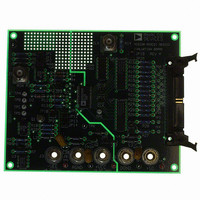
... AD9221/AD9223/AD9220 Figure 37. Evaluation Board Component Side Layout (Not to Scale) Figure 38. Evaluation Board Solder Side Layout (Not to Scale) –26– REV. E ...
Page 27
... Figure 39. Evaluation Board Ground Plane Layout (Not to Scale) REV. E Figure 40. Evaluation Board Power Plane Layout –27– AD9221/AD9223/AD9220 ...
Page 28
... AD9221/AD9223/AD9220 Figure 41. Evaluation Board Component Side Silkscreen (Not to Scale) Figure 42. Evaluation Board Component Side Silkscreen (Not to Scale) –28– REV. E ...
Page 29
... COPLANARITY 0.25 0.09 0.38 0.65 BSC 0.22 SEATING PLANE COMPLIANT TO JEDEC STANDARDS MO-150AH –29– AD9221/AD9223/AD9220 10.65 (0.4193) 10.00 (0.3937) 0.75 (0.0295) 45 0.25 (0.0098 1.27 (0.0500) 0.40 (0.0157) 8 0.95 4 0.75 0 0.55 ...
Page 30
... AD9221/AD9223/AD9220 Revision History Location 2/03—Data Sheet changed from REV REV. E. Updated graphic captions . . . . . . . . . . . . . . . . . . . . . . . . . . . . . . . . . . . . . . . . . . . . . . . . . . . . . . . . . . . . . . . . . . . . . . . . . . . . . Global Changes to DC SPECIFICATIONS . . . . . . . . . . . . . . . . . . . . . . . . . . . . . . . . . . . . . . . . . . . . . . . . . . . . . . . . . . . . . . . . . . . . . . . . . 2 Changes to ORDERING GUIDE . . . . . . . . . . . . . . . . . . . . . . . . . . . . . . . . . . . . . . . . . . . . . . . . . . . . . . . . . . . . . . . . . . . . . . . . . . . 4 Changes to INTRODUCTION . . . . . . . . . . . . . . . . . . . . . . . . . . . . . . . . . . . . . . . . . . . . . . . . . . . . . . . . . . . . . . . . . . . . . . . . . . . . . 9 Changes to Digital Output Driver Considerations (DVDD) section . . . . . . . . . . . . . . . . . . . . . . . . . . . . . . . . . . . . . . . . . . . . . . . . 21 Updated OUTLINE DIMENSIONS . . . . . . . . . . . . . . . . . . . . . . . . . . . . . . . . . . . . . . . . . . . . . . . . . . . . . . . . . . . . . . . . . . . . . . . 29 –30– Page REV. E ...
Page 31
–31– ...
Page 32
–32– ...