LM22671EVAL/NOPB National Semiconductor, LM22671EVAL/NOPB Datasheet - Page 9
LM22671EVAL/NOPB
Manufacturer Part Number
LM22671EVAL/NOPB
Description
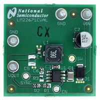
BOARD EVALUATION FOR LM22671
Manufacturer
National Semiconductor
Series
SIMPLE SWITCHER®r
Datasheets
1.LM22671MRE-ADJNOPB.pdf
(18 pages)
2.LM22671EVALNOPB.pdf
(6 pages)
3.LM22671EVALNOPB.pdf
(18 pages)
Specifications of LM22671EVAL/NOPB
Main Purpose
DC/DC, Step Down
Outputs And Type
1, Non-Isolated
Voltage - Output
3.3V
Current - Output
500mA
Voltage - Input
4.5 ~ 42 V
Regulator Topology
Buck
Frequency - Switching
500kHz
Board Type
Fully Populated
Utilized Ic / Part
LM22671
Lead Free Status / RoHS Status
Lead free / RoHS Compliant
Power - Output
-
Lead Free Status / Rohs Status
Compliant
Other names
*LM22671EVAL
*LM22671EVAL/NOPB
LM22671EVAL
LM22671EVAL
*LM22671EVAL/NOPB
LM22671EVAL
LM22671EVAL


Current Limit
When the power switch turns on, the slight capacitance load-
ing of the Schottky diode, D1, causes a leading-edge current
spike with an extended ringing period. This spike can cause
the current limit comparator to trip prematurely. A leading
edge blanking time (T
sampling the spike.
When the switch current reaches the current limit threshold
the switch is immediately turned off. If T
minimum (100 ns typical) the switcher will hold the output
current flat at the set current limit value. But if T
decreases to the minimum T
frequency decreases to 1/5 the typical frequency. This effec-
tively causes the output current to fold back to a lower and
safe value. When the current limit condition is removed the
switching frequency is restored to nominal. This 5X frequency
fold back will result in a lower duty cycle pulse of the power
switch to minimize the overall fault condition power dissipa-
tion.
The percentage of output current limit fold back is affected by
duty
See
The current limit will only protect the inductor from a runaway
condition if the LM22671 is operating in its safe operating
area. A runaway condition of the inductor is potentially catas-
trophic to the application. For every design, the safe operating
area needs to be calculated. Factors in determining the safe
operating area are the switching frequency, input voltage,
output voltage, minimum on-time and feedback voltage dur-
ing an over current condition.
As a first pass check, if the following equation holds true, a
given design is considered in a safe operating area and the
current limit will protect the circuit:
If the equation above does not hold true, the following sec-
ondary equation will need to hold true to be in safe operating
area:
Figure 2
cycle,
FIGURE 2. Output Current in Foldback vs.
for details.
V
inductance,
IN
x T
Nominal Duty Cycle
BLK
BLK
) of 100 ns (typical) is used to avoid
x F < V
ON
and
(100 ns typical) the switching
OUT
switching
x 0.724
ON
is larger than the
30076850
ON
frequency.
is at or
9
If both equations do not hold true, a particular design will not
have an effective current limit function which might damage
the circuit during startup, over current conditions, or steady
state over current and short circuit condition. Oftentimes a
reduction of the maximum input voltage or reduction of the
switching frequency will bring a design into the safe operating
area.
When synchronized to an external sync pulse, the LM22671
will not fold back the switching frequency in an over current
condition.
Soft-Start
The soft-start feature allows the regulator to gradually reach
the initial steady state operating point, thus reducing start-up
stresses and surges. The soft-start can be adjusted by se-
lecting an external soft-start capacitor. An internal 50 µA
current source charges up the external soft-start capacitor.
The generated voltage is the voltage the internal reference
limits. If no external soft-start capacitor is used, there is an
internal soft-start feature with 500 µs (typical) start-up time.
Recommended soft-start capacitor values are between 100
nF to 1 µF.
Switching Frequency Setting and
Synchronization
There are three different modes for the RT/SYNC pin. It can
be left floating for a 500 kHz switching frequency.
A resistor from the RT/SYNC pin to ground can be used to
adjust the switching frequency between 200 kHz and 1 MHz.
An external synchronization pulse can be applied to the RT/
SYNC pin for switching frequencies up to 1 MHz. The syn-
chronizing frequency must be greater than the internal switch-
ing frequency for proper operation. The maximum internal
switching frequency is guaranteed in the Electrical Charac-
teristics table. The LM22671 internally sets the RT/SYNC
mode during start up.
Many applications are limited to lower switching frequencies
due to minimum on-time and minimum off-time requirements
as well as increased switching losses at switching frequen-
cies higher than 500 kHz. In case of synchronizing to an
external sync pulse, the clock pulse must be in a valid low or
high state when the LM22671 starts up and can be applied
after device regulation. The internal oscillator will synchronize
to the external sync pulse rising edge. If the external sync
pulse is disconnected the LM22671 switching frequency will
return to default 500 kHz (typ.).
When operating at frequencies above 500 kHz, external com-
ponents such as the inductor and the output capacitors can-
not be reduced dramatically. This is due to the fixed internal
compensation and stability requirements. Running the
LM22671 at frequencies higher than 500 kHz is intended for
applications with EMI or beat frequency concerns. The flexi-
bility of increasing the switching frequency above 500 kHz can
be used to operate outside a critical signal frequency band of
an application. This can also be used to set multiple switchers
in an application to the same frequency to reduce beat fre-
quencies and simplify filtering.
See the current limit section of this datasheet for information
about the safe operating area. When synchronizing to an ex-
ternal synchronization pulse, the LM22671 will not fold back
the switching frequency in an over current condition.
The typical curve below shows adjusted switching frequen-
cies with different frequency set resistors from the RT/SYNC
pin to ground.
www.national.com
Related parts for LM22671EVAL/NOPB
Image
Part Number
Description
Manufacturer
Datasheet
Request
R

Part Number:
Description:
National Semiconductor [8-Bit D/A Converter]
Manufacturer:
National Semiconductor
Datasheet:
Part Number:
Description:
National Semiconductor [Media Coprocessor]
Manufacturer:
National Semiconductor
Datasheet:
Part Number:
Description:
Digitally Controlled Tone and Volume Circuit with Stereo Audio Power Amplifier, Microphone Preamp Stage and National 3D Sound
Manufacturer:
National Semiconductor
Datasheet:
Part Number:
Description:
Digitally Controlled Tone and Volume Circuit with Stereo Audio Power Amplifier, Microphone Preamp Stage and National 3D Sound
Manufacturer:
National Semiconductor
Datasheet:
Part Number:
Description:
AC97 Rev 2 Codec with Sample Rate Conversion and National 3D Sound
Manufacturer:
National Semiconductor
Part Number:
Description:
Manufacturer:
National Semiconductor
Datasheet:
Part Number:
Description:
Manufacturer:
National Semiconductor
Datasheet:
Part Number:
Description:
General Purpose, Low Voltage, Low Power, Rail-to-Rail Output Operational Amplifiers
Manufacturer:
National Semiconductor
Datasheet:
Part Number:
Description:
8-bit 20 MSPS flash A/D converter.
Manufacturer:
National Semiconductor
Datasheet:
Part Number:
Description:
Low Noise Quad Operational Amplifier
Manufacturer:
National Semiconductor
Datasheet:
Part Number:
Description:
Quad Differential Line Receivers
Manufacturer:
National Semiconductor
Datasheet:
Part Number:
Description:
Quad High Speed Trapezoidal? Bus Transceiver
Manufacturer:
National Semiconductor
Datasheet:
Part Number:
Description:
Dual Line Receiver
Manufacturer:
National Semiconductor
Datasheet:
Part Number:
Description:
TTL to 10k ECL Level Translator with Latch
Manufacturer:
National Semiconductor
Datasheet: