DR3101 RFM, DR3101 Datasheet

RF Receiver 2G Transceiver Module 315 MHz

DR3101

Manufacturer Part Number
DR3101
Description
RF Receiver 2G Transceiver Module 315 MHz
Manufacturer
RFM
Type
Transceiverr
Datasheet

Specifications of DR3101

Operating Frequency
315.2 MHz
Operating Supply Voltage
3.3 V
Maximum Operating Temperature
+ 85 C
Minimum Operating Temperature
- 40 C
Lead Free Status / RoHS Status
Lead free / RoHS Compliant
· Designed for Short-Range Wireless Data Communications
· Supports 2.4-19.2 kbps Encoded Data Transmissions
· 3 V, Low Current Operation plus Sleep Mode
· Ready to Use OEM Module
The DR3101 transceiver module is ideal for short-range wireless data applications where robust
operation, small size and low power consumption are required. The DR3101 utilizes RFM’s
TR3001 amplifier-sequenced hybrid (ASH) architecture to achieve this unique blend of charac-
teristics. The receiver section of the TR3001 is sensitive and stable. A wide dynamic range log
detector provides robust performance in the presence of on-channel interference or noise. Two
stages of SAW filtering provide excellent receiver out-of-band rejection. The transmitter includes
provisions for both on-off keyed (OOK) and amplitude-shift keyed (ASK) modulation. The trans-
mitter employs SAW filtering to suppress output harmonics, facilitating compliance with FCC
Part 15 and similar regulations. The DR3101 includes the TR3001 plus all configuration compo-
nents in a ready-to-use PCB assembly, excellent for prototyping and intermediate volume pro-
duction runs.
Electrical Characteristics, 2.4 kbps On-Off Keyed
Absolute Maximum Ratings
Power Supply and All Input/Output Pins
Non-Operating Case Temperature
Soldering Temperature (10 seconds)
Operating Frequency
Modulation Type
Data Rate
Receiver Performance (OOK @ 2.4 kbps)
Transmitter Performance (OOK @ 2.4 kbps)
Sleep to Receive Switch Time (100 ms sleep, -85 dBm signal)
Sleep Mode Current
Transmit to Receive Switch Time (100 ms transmit, -85 dBm signal)
Receive to Transmit Switch Time
Power Supply Voltage Range
Operating Ambient Temperature
®
Input Current, 3 Vdc Supply
Input Signal for 10
Rejection, ±30 MHz
Peak Input Current, 3 Vdc Supply
Peak Output Power
Turn On/Turn Off Time
Characteristic
Rating
-4
BER, 25 C
1
t
ON
Sym
R
t
t
-0.3 to +4.0
-50 to +100
V
I
P
t
TOR
RTO
T
f
I
/t
SR
I
REJ
TP
O
R
S
CC
O
A
OFF
Value
230
Notes
Units
o
o
Minimum
V
C
C
314.80
2.7
-40
55
Transceiver
Typical
315.00 MHz
OOK
-100
0.75
0.75
200
200
2.4
DR3101
DEVELOPMENT KIT
Module
(Info
Click
Maximum
315.20
12/6
+85
4.5
3.5
12
12
here)
Units
MHz
kbps
dBm
mW
Vdc
mA
mA
dB
µA
µs
µs
µs
µs
o
C

Related parts for DR3101

DR3101 Summary of contents

Page 1

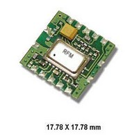
... The trans- mitter employs SAW filtering to suppress output harmonics, facilitating compliance with FCC Part 15 and similar regulations. The DR3101 includes the TR3001 plus all configuration compo- nents in a ready-to-use PCB assembly, excellent for prototyping and intermediate volume pro- duction runs ...

Page 2

2 ...

Page 3

Pin Descriptions Pin Name This pin is connected directly to the transceiver AGCCAP pin. To disable AGC operation, this pin is tied to VCC. To enable AGC operation, a capacitor is placed between this pin and ground. This pin controls ...

Page 4

GND This is a ground pin. 7 GND This is a ground pin. This pin is the receiver low-pass filter bandwidth adjust, and is connected directly to the transceiver LPFADJ pin the circuit board (330 K) is ...

Page 5

... Inductor Chip 0805CS Inductor Chip 0805CS Printed Circuit Board 5 Value Quantity 315.00 MHz 1 100 pF ±10% 4 0.1 µF ±10% 1 4.7 µF ±10% 1 270 K ±5% 1 330 K ± ±1% 1 100 K ±1% 1 4.7 K ±5% 1 330 K ±5% 1 zero ohm jumper 1 N ± ±10% 1 400-1526-001X1 1 file: dr3101i.vp, 2002.10.23 rev ...

Related keywords