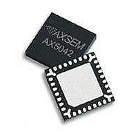
AX5043-QFN28-TU AXSEM, AX5043-QFN28-TU Datasheet - Page 57

AX5043-QFN28-TU
Manufacturer Part Number
AX5043-QFN28-TU
Description
RF Transceiver Narrow-Band-IC
Manufacturer
AXSEM
Datasheet
1.AX5043-QFN28-TU.pdf
(60 pages)
Specifications of AX5043-QFN28-TU
Number Of Receivers
1
Number Of Transmitters
1
Wireless Frequency
70 MHz to 1050 MHz
Interface Type
SPI
Output Power
18 dBm to 22 dBm
Operating Supply Voltage
1.8 V to 3.6 V
Maximum Operating Temperature
+ 85 C
Maximum Supply Current
60 mA
Minimum Operating Temperature
- 40 C
Modulation
ASK, FSK
Lead Free Status / RoHS Status
Lead free / RoHS Compliant
8.3.
1.
Figure 18: PCB land and solder mask recommendations
2.
3.
8.4.
Stencil Design & Solder Paste Application
1.
2.
3.
4.
5.
6.
7.
Version 0.2
PCB land and solder masking recommendations are shown in Figure 18.
Thermal vias should be used on the PCB thermal pad (middle ground pad) to improve thermal
conductivity from the device to a copper ground plane area on the reverse side of the printed
circuit board. The number of vias depends on the package thermal requirements, as
determined by thermal simulation or actual testing.
Increasing the number of vias through the printed circuit board will improve the thermal
conductivity to the reverse side ground plane and external heat sink. In general, adding more
metal through the PC board under the IC will improve operational heat transfer, but will
require careful attention to uniform heating of the board during assembly.
Stainless steel stencils are recommended for solder paste application.
A stencil thickness of 0.125 – 0.150 mm (5 – 6 mils) is recommended for screening.
For the PCB thermal pad, solder paste should be printed on the PCB by designing a stencil with
an array of smaller openings that sum to 50% of the QFN exposed pad area. Solder paste
should be applied through an array of squares (or circles) as shown in Figure 19.
The aperture opening for the signal pads should be between 50-80% of the QFN pad area as
shown in Figure 20.
Optionally, for better solder paste release, the aperture walls should be trapezoidal and the
corners rounded.
The fine pitch of the IC leads requires accurate alignment of the stencil and the printed circuit
board. The stencil and printed circuit assembly should be aligned to within + 1 mil prior to
application of the solder paste.
No-clean flux is recommended since flux from underneath the thermal pad will be difficult to
clean if water-soluble flux is used.
QFN28 Recommended Pad Layout
Assembly Process
Preliminary
QFN28 Package Information
Datasheet AX5043
57


