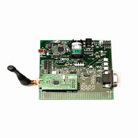
EVAL-ADF70XXEKZ1 Analog Devices Inc, EVAL-ADF70XXEKZ1 Datasheet - Page 10
EVAL-ADF70XXEKZ1
Manufacturer Part Number
EVAL-ADF70XXEKZ1
Description
KIT DEV ADF702X FOR BF533EZKIT
Manufacturer
Analog Devices Inc
Type
Transceiver, ISMr
Specifications of EVAL-ADF70XXEKZ1
Frequency
431MHz ~ 464MHz, 862MHz ~ 870MHz, 902MHz ~ 928MHz
For Use With/related Products
ADF702x
For Use With
EVAL-ADF70XXMBZ2 - MOTHER BOARD FOR ADISIMLINK DEV
Lead Free Status / RoHS Status
Lead free / RoHS Compliant


ADF7025
PIN CONFIGURATION AND FUNCTION DESCRIPTIONS
Table 4. Pin Function Descriptions
Pin No.
1
2
3
4
5
6
7
8
9
10
11
12
13 to 18
19, 22
20, 21, 23
24
25
26
27
28
Mnemonic
VCOIN
VREG1
VDD1
RFOUT
RFGND
RFIN
RFINB
R
VDD4
RSET
VREG4
GND4
MIX/FILT
GND4
FILT/TEST_A
CE
SLE
SDATA
SREAD
SCLK
LNA
Voltage supply for LNA/MIXER Block. This pin should be decoupled to ground with a 10 nF capacitor.
Signal Chain Test Pins. These pins are high impedance under normal conditions and should be left unconnected.
Signal Chain Test Pins. These pins are high impedance under normal conditions and should be left unconnected.
Description
The tuning voltage on this pin determines the output frequency of the voltage-controlled oscillator (VCO).
The higher the tuning voltage, the higher the output frequency.
Regulator Voltage for PA Block. A 100 nF in parallel with a 5.1 pF capacitor should be placed between this pin
and ground for regulator stability and noise rejection.
Voltage Supply for PA Block. Decoupling capacitors of 0.1 µF and 10 pF should be placed as close as possible
to this pin. All VDD pins should be tied together.
The modulated signal is available at this pin. Output power levels are from −20 dBm to +13 dBm. The output
should be impedance-matched to the desired load using suitable components. See the Transmitter section.
Ground for Output Stage of Transmitter.
LNA Input for Receiver Section. Input matching is required between the antenna and the differential LNA
input to ensure maximum power transfer. See the LNA/PA Matching section.
Complementary LNA Input. See the LNA/PA Matching section.
External bias resistor for LNA. Optimum resistor is 1.1 kΩ with 5% tolerance.
External Resistor to Set Charge Pump Current and Some Internal Bias Currents. Use 3.6 kΩ with 5% tolerance.
Regulator Voltage for LNA/MIXER Block. A 100 nF capacitor should be placed between this pin and GND
for regulator stability and noise rejection.
Ground for LNA/MIXER Block.
Ground for LNA/MIXER Block.
Chip Enable. Bringing CE low puts the ADF7025 into complete power-down. Register values are lost
when CE is low, and the part must be reprogrammed once CE is brought high.
Load Enable, CMOS Input. When LE goes high, the data stored in the shift registers is loaded into one
of the four latches. A latch is selected using the control bits.
Serial Data Input. The serial data is loaded MSB first with the two LSBs as the control bits. This pin is
a high impedance CMOS input.
Serial Data Output. This pin is used to feed readback data from the ADF7025 to the microcontroller.
The SCLK input is used to clock each readback bit (ADC readback) from the SREAD pin.
Serial Clock Input. This serial clock is used to clock in the serial data to the registers. The data is latched
into the 24-bit shift register on the CLK rising edge. This pin is a digital CMOS input.
RFGND
RFOUT
VREG1
VREG4
VCOIN
RFINB
GND4
VDD1
VDD4
RSET
RFIN
R
LNA
10
11
12
1
2
3
4
5
6
7
8
9
PIN 1
INDICATOR
Figure 5. Pin Configuration
Rev. A | Page 10 of 44
(Not to Scale)
ADF7025
TOP VIEW
36
35
34
33
32
31
30
29
28
27
26
25
CLKOUT
DATA CLK
DATA I/O
INT/LOCK
VDD2
VREG2
ADCIN
GND2
SCLK
SREAD
SDATA
SLE
Related parts for EVAL-ADF70XXEKZ1
Image
Part Number
Description
Manufacturer
Datasheet
Request
R

Part Number:
Description:
IC, ADJ LDO REG, 1.5V TO 5V 250mA MSOP-8
Manufacturer:
Vishay
Datasheet:

Part Number:
Description:
IC, ADJ LDO REG, 1.5V TO 5V 0.6A 8-TSSOP
Manufacturer:
Vishay
Datasheet:
Part Number:
Description:
IC, ADJ LDO REG, 1.5V TO 5V 250mA MSOP-8
Manufacturer:
Vishay
Datasheet:

Part Number:
Description:
IC ADJ LDO REG 1.5V TO 5V 150mA 5-SOT-23
Manufacturer:
Vishay
Datasheet:

Part Number:
Description:
BOARD EVAL AS1324-AD
Manufacturer:
austriamicrosystems
Datasheet:
Part Number:
Description:
IC, ADJ LDO REG, 1.5V TO 5V 0.6A 8-TSSOP
Manufacturer:
Vishay
Datasheet:

Part Number:
Description:
IC, ADJ LDO REG, 1.5V TO 5V, 0.3A, MSOP8
Manufacturer:
Vishay
Datasheet:
Part Number:
Description:
IC, ADJ LDO REG, 1.5V TO 5V, 0.3A, MSOP8
Manufacturer:
Vishay
Datasheet:
Part Number:
Description:
IC, ADJ LDO REG 1.215V TO 5V 0.3A MSOP-8
Manufacturer:
Vishay
Datasheet:
Part Number:
Description:
IC, ADJ LDO REG 1.215V TO 5V 0.3A MSOP-8
Manufacturer:
Vishay
Datasheet:

Part Number:
Description:
±1.7g Dual-Axis IMEMS Accelerometer Evaluation Board
Manufacturer:
Analog Devices Inc
Datasheet:

Part Number:
Description:
IC MULTIPLIER ANALOG 8-SOIC T/R
Manufacturer:
Analog Devices Inc
Datasheet:

Part Number:
Description:
IC ANALOG MULTIPLIER 8-DIP
Manufacturer:
Analog Devices Inc
Datasheet:
Part Number:
Description:
IC ANALOG MULTIPLIER 8-SOIC
Manufacturer:
Analog Devices Inc
Datasheet:
Part Number:
Description:
IC ANALOG MULTIPLIER 8-DIP
Manufacturer:
Analog Devices Inc
Datasheet: