ADIS16201CCCZ Analog Devices Inc, ADIS16201CCCZ Datasheet - Page 19
ADIS16201CCCZ
Manufacturer Part Number
ADIS16201CCCZ
Description
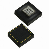
IC ACCELEROMETER LP 16-LGA
Manufacturer
Analog Devices Inc
Datasheet
1.ADIS16201PCBZ.pdf
(32 pages)
Specifications of ADIS16201CCCZ
Acceleration Range
±1.7g
Axis
X, Y
Sensitivity
2.162 LSB/mg
Voltage - Supply
3 V ~ 3.6 V
Output Type
Digital
Bandwidth
2.25kHz
Interface
SPI
Mounting Type
Surface Mount
Package / Case
16-LGA
No. Of Axes
2
Sensor Case Style
LGA
No. Of Pins
16
Supply Voltage Range
3V To 3.6V
Operating Temperature Range
-40°C To +125°C
Msl
MSL 1 - Unlimited
Lead Free Status / RoHS Status
Lead free / RoHS Compliant
For Use With
ADIS16201/PCBZ - BOARD EVAL PCB ADIS16201
Lead Free Status / RoHS Status
Lead free / RoHS Compliant, Lead free / RoHS Compliant
Available stocks
Company
Part Number
Manufacturer
Quantity
Price
Company:

Part Number:
ADIS16201CCCZ
Manufacturer:
IXYS
Quantity:
3 000
Part Number:
ADIS16201CCCZ
Manufacturer:
ADI原装
Quantity:
20 000


CONTROL REGISTER DETAILS
The control registers in the ADIS16201 are 16 bits in length.
Each of them has been assigned an address for their upper byte
and lower byte. The bit map of each control register uses the
numerical assignments that are displayed in the following table.
MSB
15
7
The upper byte consists of Bit 8 to Bit 15, and the lower byte
consists of Bit 0 to Bit 7. Each of the following sections provides
a description of each register that includes purpose, relevant
scaling information, bit maps, addresses, and default values.
CALIBRATION
The ADIS16201 outputs are precalibrated at the factory, providing
a high degree of accuracy and simpler system implementation.
In addition, for system or field updates, the device has eight
control registers associated with calibrating the acceleration and
inclination output data (see the Calibration Register Definitions
section). Each of these registers has read/write capability and is
16 bits (2 bytes) in length. All calibration registers are 12 bits in
length, with the exception of the inclination offset registers, which
are 9 bits in length. All data values are aligned to the LSB. The
OFFSET registers all utilize the twos complement format
allowing for both positive and negative offsets. All scale registers
utilize the straight binary format.
The data within these eight calibration registers is utilized in
offsetting and scaling of the output data registers according to
the following relationship:
where:
x represents the raw data prior to calibration.
C is the offset.
A is the scalar.
Output represents the output data register where the resultant
data is stored.
All four inertial sensor outputs (X and Y acceleration, X and Y
inclination) have their own independent set of calibration
registers.
Simple access to these registers enables field calibration to
correct for in-system error sources. In particular, the offset
control registers allow the user to reset to 0°/0 m g reference
point for the device. This is particularly important when
considering the stack-up of the tolerances in mounting the
ADIS16201 to a printed circuit board (PCB), the PCB to an
enclosure, the enclosure mounted to the chassis of a piece of
equipment, and so on.
Output
14
6
=
A
13
5
×
(
x
+
C
)
12
4
11
3
10
2
9
1
8
0
LSB
Rev. A | Page 19 of 32
The result is that the ADIS16201 mechanical reference can be
offset several degrees from that of the end equipment
mechanical reference, resulting in an accumulation of offset
errors in the inclination and acceleration data output registers.
The offset registers provide a convenient tool for managing
these types of errors.
A global command is implemented within the ADIS16201 to
simplify the loading of the offsets. Once the end piece of
equipment is leveled to its desired reference point, a null
command can be sent to the ADIS16201 via the command
control register, which zeros the two acceleration and the two
inclination output data registers. This command loads all four
offset registers with the inverse of their contents at the time of
the null command. Consequently, on the next reading of the
seven output data registers, the two acceleration and two
inclination output data registers should be reset to mid-scale
(neglecting noise and repeatability limitations). It is suggested
that when the null command is implemented, the AVG_CNT
control register be set to 08h in order to maximize the filtering
and reduce the effects of noise in determining the values to be
loaded into the offset control registers. Optionally, the user can
manually load each of the eight calibration registers via the SPI
in order to calibrate the end system. This is applicable when the
user plans to adjust the scale factors, thus requiring an external
stimulus to excite the ADIS16201.
CALIBRATION REGISTER DEFINITIONS
XACCL_OFF Register Definition
Address
0x11, 0x10
1
The XACCL_OFF register is the user-controlled register for
calibrating system-level acceleration offset errors. For the X-axis
acceleration, it represents the C variable in the calibration
equation. The maximum calibration range is +0.945 g , or
+2047/−2048 codes, assuming nominal sensor sensitivity. The
contents of this register are nonvolatile.
Table 11. XACCL_OFF Bit Designations
Bit
15:12
11:0
Scale is the weight of each LSB.
Description
Not used
Data bits
Scale
0.4624 mg
1
Default
0x0000
Format
Twos
complement
ADIS16201
Access
R/W
Related parts for ADIS16201CCCZ
Image
Part Number
Description
Manufacturer
Datasheet
Request
R

Part Number:
Description:
±1.7g Dual-Axis IMEMS Accelerometer Evaluation Board
Manufacturer:
Analog Devices Inc
Datasheet:

Part Number:
Description:
Inertial Sensor Evaluation System
Manufacturer:
Analog Devices Inc
Datasheet:
Part Number:
Description:
Manufacturer:
Analog Devices Inc
Datasheet:
Part Number:
Description:
Manufacturer:
Analog Devices Inc
Datasheet:
Part Number:
Description:
Manufacturer:
Analog Devices Inc
Datasheet:
Part Number:
Description:
Manufacturer:
Analog Devices Inc
Datasheet:
Part Number:
Description:
Manufacturer:
Analog Devices Inc
Datasheet:
Part Number:
Description:
Manufacturer:
Analog Devices Inc
Datasheet:
Part Number:
Description:
Manufacturer:
Analog Devices Inc
Datasheet:
Part Number:
Description:
Manufacturer:
Analog Devices Inc
Datasheet:
Part Number:
Description:
Manufacturer:
Analog Devices Inc
Datasheet:
Part Number:
Description:
Manufacturer:
Analog Devices Inc
Datasheet:
Part Number:
Description:
Manufacturer:
Analog Devices Inc
Datasheet: