LIS3DHTR STMicroelectronics, LIS3DHTR Datasheet
LIS3DHTR
Specifications of LIS3DHTR
Available stocks


Related parts for LIS3DHTR


LIS3DHTR Summary of contents
Page 1
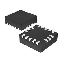
... LIS3DH is available in small thin plastic land grid array package (LGA) and it is guaranteed to operate over an extended temperature range from -40 °C to +85 °C. Table 1. Device summary Temp. Order codes range [°C] LIS3DH -40 to +85 LIS3DHTR -40 to +85 Doc ID 17530 Rev 1 LIS3DH 2 C/SPI Package Packaging LGA-16 Tray LGA-16 Tape and reel 1/42 www ...
Page 2
Contents Contents 1 Block diagram and pin description . . . . . . . . . . . . . . . . . . . . . . . . . . . . . 8 1.1 Block ...
Page 3
LIS3DH 5.1.2 5.1.3 5.1.4 5.1.5 6 Digital interfaces . . . . . . . . . . . . . . . . . . . . . . . . . . . . . . . . ...
Page 4
Contents 8.20 FIFO_SRC_REG (2Fh ...
Page 5
LIS3DH List of figures Figure 1. Block diagram . . . . . . . . . . . . . . . . . . . . . . . . . . . . . . . . ...
Page 6
List of tables List of tables Table 1. Device summary . . . . . . . . . . . . . . . . . . . . . . . . . . . . . . ...
Page 7
LIS3DH Table 49. INT1_SRC register . . . . . . . . . . . . . . . . . . . . . . . . . . . . . . . . . . . ...
Page 8
Block diagram and pin description 1 Block diagram and pin description 1.1 Block diagram Figure 1. Block diagram a ADC1 - ADC Input1 ADC2 - ADC Input2 ADC3 - ADC Input3 SELF TEST 1.2 Pin description Figure 2. Pin connection ...
Page 9
LIS3DH Table 2. Pin description Pin Name Vdd_IO Power supply for I/O pins NC Not connected NC Not connected 2 SCL I C serial ...
Page 10
Mechanical and electrical specifications 2 Mechanical and electrical specifications 2.1 Mechanical characteristics Vdd = 2 °C unless otherwise noted Table 3. Mechanical characteristics Symbol Parameter (2) FS Measurement range So Sensitivity Sensitivity change vs TCSo temperature ...
Page 11
LIS3DH 2.2 Temperature sensor characteristics Vdd =2.5 V, T=25 °C unless otherwise noted Table 4. Temperature sensor characteristics Symbol Parameter Temperature sensor output change vs TSDr temperature TODR Temperature refresh rate Top Operating temperature range 1. Typical specifications are not ...
Page 12
Mechanical and electrical specifications 2.4 Communication interface characteristics 2.4.1 SPI - serial peripheral interface Subject to general operating conditions for Vdd and Top. Table 6. SPI slave timing values Symbol tc(SPC) SPI clock cycle fc(SPC) SPI clock frequency tsu(CS) CS ...
Page 13
LIS3DH 2 2.4 Inter IC control interface Subject to general operating conditions for Vdd and top. 2 Table slave timing values Symbol Parameter f SCL clock frequency (SCL) t SCL clock low time w(SCLL) ...
Page 14
Mechanical and electrical specifications 2.5 Absolute maximum ratings Stresses above those listed as “absolute maximum ratings” may cause permanent damage to the device. This is a stress rating only and functional operation of the device under these conditions is not ...
Page 15
LIS3DH 3 Terminology and functionality 3.1 Terminology 3.1.1 Sensitivity Sensitivity describes the gain of the sensor and can be determined e.g. by applying 1 g acceleration to it. As the sensor can measure DC accelerations this can be done easily ...
Page 16
Terminology and functionality 3.2.2 Self-test Self-test allows to check the sensor functionality without moving it. The self-test function is off when the self-test bit (ST) is programmed to ‘0‘. When the self-test bit is programmed to ‘1‘ an actuation force ...
Page 17
LIS3DH 3.5 Factory calibration The IC interface is factory calibrated for sensitivity (So) and Zero-g level (TyOff). The trimming values are stored inside the device in a non volatile memory. Any time the device is turned on, the trimming parameters ...
Page 18
Application hints 4 Application hints Figure 5. LIS3DH electrical connection Vdd Digital signal from/to signal controller.Signal’s levels are defined by proper selection of Vdd_IO The device core is supplied through Vdd line while the I/O pads are supplied through Vdd_IO ...
Page 19
LIS3DH 5 Digital main blocks 5.1 FIFO LIS3DH embeds a 32-slot of 10bit data FIFO for each of the three output channels and Z. This allows a consistent power saving for the system, since the host processor does ...
Page 20
Digital interfaces 6 Digital interfaces The registers embedded inside the LIS3DH may be accessed through both the I serial interfaces. The latter may be SW configured to operate either in 3-wire or 4-wire interface mode. The serial interfaces are mapped ...
Page 21
... LSb is ‘1’ (address 0011001b) else if SA0 pad is connected to ground, LSb value is ‘0’ (address 0011000b). This solution permits to connect and address two different accelerometers to the same I Data transfer with acknowledge is mandatory. The transmitter must release the SDA line during the acknowledge pulse. The receiver must then pull the data line LOW so that it remains stable low during the HIGH period of the acknowledge clock pulse ...
Page 22
Digital interfaces Table 15. Transfer when master is receiving (reading) one byte of data from slave: Master ST SAD + W Slave Table 16. Transfer when master is receiving (reading) multiple bytes of data from slave Master ST SAD+W SUB ...
Page 23
LIS3DH SDO are respectively the serial port data input and output. Those lines are driven at the falling edge of SPC and should be captured at the rising edge of SPC. Both the read register and write register commands are ...
Page 24
Digital interfaces Figure 8. Multiple bytes SPI read protocol (2 bytes example) CS SPC SDI RW MS SDO 6.2.2 SPI write Figure 9. SPI write protocol CS SPC SDI The SPI Write command is performed with 16 clock pulses. Multiple ...
Page 25
LIS3DH 6.2.3 SPI read in 3-wires mode 3-wires mode is entered by setting to ‘1’ bit SIM (SPI serial interface mode selection) in CTRL_REG4. Figure 11. SPI read protocol in 3-wires mode CS SPC SDI/O The SPI read command is ...
Page 26
Register mapping 7 Register mapping The table given below provides a listing of the 8 bit registers embedded in the device and the related addresses: Table 17. Register address map Name Reserved (do not modify) STATUS_REG_AUX OUT_ADC1_L OUT_ADC1_H OUT_ADC2_L OUT_ADC2_H ...
Page 27
LIS3DH Table 17. Register address map Name INT1_SOURCE INT1_THS INT1_DURATION Reserved CLICK_CFG CLICK_SRC CLICK_THS TIME_LIMIT TIME_LATENCY TIME_WINDOW Registers marked as Reserved must not be changed. The writing to those registers may cause permanent damages to the device. The content of ...
Page 28
Registers description 8 Registers description 8.1 STATUS_AUX (07h) Table 18. STATUS_REG_AUX register 321OR 3OR Table 19. STATUS_REG_AUX description 321OR 1, 2 and 3 axis data overrun. Default value: 0 (0: no overrun has occurred new set of data ...
Page 29
LIS3DH 8.5 INT_COUNTER (0Eh) Table 20. INT_COUNTER register IC7 IC6 8.6 WHO_AM_I (0Fh) Table 21. WHO_AM_I register 0 0 Device identification register. 8.7 TEMP_CFG_REG (1Fh) Table 22. TEMP_CFG_REG register ADC_PD TEMP_EN Table 23. TEMP_CFG_REG description ADC enable. Default value: 0 ...
Page 30
Registers description ODR<3:0> is used to set power mode and ODR selection. In the following table are reported all frequency resulting in combination of ODR<3:0> Table 26. Data rate configuration ODR3 ODR2 ...
Page 31
LIS3DH Table 29. High pass filter mode configuration HPM1 HPM0 8.10 CTRL_REG3 (22h) Table 30. CTRL_REG3 register I1_CLICK I1_AOI1 Table 31. CTRL_REG3 description I1_CLICK I1_AOI1 I1_AOI2 I1_DRDY1 I1_DRDY2 I1_WTM I1_OVERRUN 8.11 CTRL_REG4 ...
Page 32
Registers description Table 33. CTRL_REG4 description (continued) HR ST1-ST0 SIM Table 34. Self test mode configuration ST1 8.12 CTRL_REG5 (24h) Table 35. CTRL_REG5 register BOOT FIFO_EN Table 36. CTRL_REG5 description BOOT FIFO_EN LIR_INT1 D4D_INT1 8.13 CTRL_REG6 ...
Page 33
LIS3DH Table 39. REFERENCE register description Ref 7-Ref0 8.15 STATUS_REG (27h) Table 40. STATUS register ZYXOR ZOR Table 41. STATUS register description ZYXOR X, Y and Z axis data overrun. Default value: 0 (0: no overrun has occurred ...
Page 34
Registers description 8.19 FIFO_CTRL_REG (2Eh) Table 42. REFERENCE register FM1 FM0 Table 43. REFERENCE register description FM1-FM0 FIFO mode selection. Default value: 00 (see TR Trigger selection. Default value Trigger event liked to trigger signal on INT1 1: ...
Page 35
LIS3DH Table 47. INT1_CFG description ZLIE/ Enable interrupt generation on Z low event or on Direction recognition. Default ZDOWNE value: 0 (0: disable interrupt request;1: enable interrupt request) YHIE/ Enable interrupt generation on Y high event or on Direction recognition. ...
Page 36
Registers description Table 50. INT1_SRC description Y low. Default value (0: no interrupt Low event has occurred) X high. Default value (0: no interrupt High event has occurred) X low. Default value: ...
Page 37
LIS3DH Table 56. CLICK_CFG description 8.26 CLICK_SRC (39h) Table 57. CLICK_SRC register IA Table 58. CLICK_SRC description - - IA Interrupt active. Default value: 0 (0: no interrupt has been generated; 1: one or ...
Page 38
Registers description 8.27 CLICK_THS (3Ah) Table 59. CLICK_THS register - Ths6 Table 60. CLICK_SRC description Ths6-Ths0 8.28 TIME_LIMIT (3Bh) Table 61. TIME_LIMIT register - TLI6 Table 62. TIME_LIMIT description TLI7-TLI0 8.29 TIME_LATENCY (3Ch) Table 63. TIME_LATENCY register TLA7 TLA6 Table ...
Page 39
LIS3DH 9 Package information In order to meet environmental requirements, ST offers these devices in different grades of ® ECOPACK packages, depending on their level of environmental compliance. ECOPACK specifications, grade definitions and product status are available at: ECOPACK is ...
Page 40
Package information Table 67. LGA-16: Mechanical data Dim Figure 12. LGA-16: Mechanical data and package dimensions 40/42 mm Min. Typ. 0.785 0.2 2.85 3 ...
Page 41
LIS3DH 10 Revision history Table 68. Document revision history Date 21-May-2010 Revision 1 Initial release Doc ID 17530 Rev 1 Revision history Changes 41/42 ...
Page 42
... Information in this document is provided solely in connection with ST products. STMicroelectronics NV and its subsidiaries (“ST”) reserve the right to make changes, corrections, modifications or improvements, to this document, and the products and services described herein at any time, without notice. All ST products are sold pursuant to ST’s terms and conditions of sale. ...