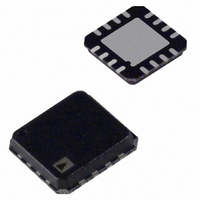
ADA4856-3YCPZ-R2 Analog Devices Inc, ADA4856-3YCPZ-R2 Datasheet

ADA4856-3YCPZ-R2
Specifications of ADA4856-3YCPZ-R2
Related parts for ADA4856-3YCPZ-R2
ADA4856-3YCPZ-R2 Summary of contents
Page 1
... V below the positive rail. In addition, the output voltage swings within 200 mV of either supply, making this video amplifier easy to use on single-supply voltages as low as 3.3 V. The ADA4856-3 offers a typical low power of 7.8 mA per amplifier, while being capable of delivering load current. It also features a power-down function for power sensitive applications that reduces the supply current ...
Page 2
... Initial Version Theory of Operation ...................................................................... 12 Applications Information .............................................................. 13 Using the ADA4856-3 in Gains Equal to +1, −1 ........................ 13 Using the ADA4856-3 in Gains Equal to +3, +4, and +5 ..... 14 20 MHz Active Low-Pass Filter ................................................ 15 Video Line Driver ....................................................................... 15 Single-Supply Operation ........................................................... 16 Power Down ................................................................................ 16 ...
Page 3
... V p- kΩ MHz f = 100 kHz f = 100 kHz V = −0 HD2 ≤ −60 dBc Ω L Enabled Powered down ∆ Rev Page ADA4856-3 Min Typ Max 370 225 200 90 74 800 4.8/5.2 −92/−110 −68/−71 − 0.01 0.01 1.3 3.4 5.5 − ...
Page 4
... ADA4856-3 3.3 V OPERATION T = 25° 3.3 V, − + Table 2. Parameter DYNAMIC PERFORMANCE −3 dB Bandwidth Bandwidth for 0.1 dB Flatness Slew Rate Settling Time to 0.1% (Rise/Fall) NOISE/DISTORTION PERFORMANCE Harmonic Distortion (HD2/HD3) Crosstalk, Output to Output Input Voltage Noise Input Current Noise Differential Gain Error Differential Phase Error ...
Page 5
... JA 16-Lead LFCSP 67 MAXIMUM POWER DISSIPATION The maximum power that can be safely dissipated by the Rating ADA4856-3 is limited by the associated rise in junction 6 V temperature. The maximum safe junction temperature for See Figure 3 plastic encapsulated devices is determined by the glass transition (−V − 0 (+V − ...
Page 6
... S 10 −IN2 11 OUT2 − OUT1 15 −IN1 16 +IN1 17 (EPAD) Exposed Pad (EPAD ADA4856-3 +IN2 2 TOP VIEW (Not to Scale NOTES CONNECT. 2. EXPOSED PAD CONNECTED TO –V Figure 4. Pin Configuration Description No Connect. Noninverting Input 2. No Connect. Power Down. Noninverting Input 3. Inverting Input 3. Output 3. Negative Supply. ...
Page 7
... T = +105° –40° +85°C A –4 –6 – 100 FREQUENCY (MHz) Figure 9. Small Signal Frequency Response vs. Temperature C = 4.4pF 2.2pF –2 –4 – 100 FREQUENCY (MHz) Figure 10. Small Signal Frequency Response vs. Capacitive Load ADA4856-3 = 1.4V p-p OUT 1000 1000 C = 6.6pF L 1000 ...
Page 8
... ADA4856-3 – 1kΩ L – p-p OUT –70 –80 –90 –100 HD2 –110 –120 –130 –140 0.1 1 FREQUENCY (MHz) Figure 11. Harmonic Distortion vs. Frequency 0 –20 –40 OUT3 –60 –80 OUT2 –100 –120 0 FREQUENCY (MHz) Figure 12. Forward Isolation vs. Frequency 0 –10 –20 –30 –40 –50 +PSRR – ...
Page 9
... Figure 21. Large Signal Transient Response vs. Supply Voltage 1.5 1.0 0.5 0 –0.5 –1.0 –1.5 Figure 22. Large Signal Transient Response vs. Capacitive Load Rev Page ADA4856-3 100 1k 10k 100k FREQUENCY (Hz) Figure 20. Output Current Noise vs. Frequency TIME (10ns/DIV 2.2pF 4.4pF ...
Page 10
... ADA4856-3 0.08 0.06 0.04 0.02 0 –0.02 –0.04 –0. 3.3V S –0.08 TIME (10ns/DIV) Figure 23. Small Signal Transient Response vs. Capacitive Load 4 2 × OUT 1 0 –1 –2 –3 –4 TIME (50ns/DIV) Figure 24. Output Overdrive Recovery 3 2.5 2.0 1.5 V 1.0 0.5 0 –0.5 –1.0 –1.5 TIME (1us/DIV) Figure 25 ...
Page 11
... Figure 31. Output Saturation Voltage vs. Load Current 25.0 24.5 24.0 23.5 23.0 22.5 22.0 2.7 1G Figure 32. Quiescent Current vs. Supply Voltage Rev Page ADA4856-3 0 LOAD CURRENT (mA) 3.0 3.3 3.6 3.9 4.2 4.5 4.8 5.1 SUPPLY VOLTAGE (V) 100 5.4 ...
Page 12
... ADA4856-3 ideal for low voltage single-supply applications. In addition, this new input stage does not sacrifice noise performance for slew rate nV/√Hz, the ADA4856-3 is one of the lowest noise rail-to-rail output video amplifiers in the market. Besides a novel input stage, the ADA4856-3 employs the Analog Devices, Inc ...
Page 13
... Whereas the ADA4856-3 has a fixed gain +2, it can be used in other gain configurations, such −1 and G = +1. Unity-Gain Operation Option 1 There are two options for obtaining unity gain (G = +1) ...
Page 14
... Gain of +3 Configuration Figure 38 shows the ADA4856-3 used as an amplifier with a fixed gain of +3. No external resistors are required, just a simple trace connecting certain inputs and outputs. Connect V which is set to a gain of +2, and U2, which is set to unity. U3 then ...
Page 15
... FREQUENCY (MHz) Figure 43. 20 MHz, Low-Pass Filter Frequency Response VIDEO LINE DRIVER The ADA4856-3 was designed to excel in video driver applications. Figure 44 shows a typical schematic for a video driver operating on bipolar supplies (G) IN OUT2 V IN – In applications that require multiple video loads be driven ...
Page 16
... POWER SUPPLY BYPASSING Careful attention must be paid to bypassing the power supply pins of the ADA4856-3. Use high quality capacitors with low equivalent series resistance (ESR), such as multilayer ceramic capacitors (MLCCs), to minimize supply voltage ripple and power dissipation. A large, usually tantalum, 10 μ μF capacitor located in ...
Page 17
... OUTLINE DIMENSIONS PIN 1 INDICATOR 12° MAX 1.00 0.85 0.80 ORDERING GUIDE Model Temperature Range 1 ADA4856-3YCPZ-R2 –40°C to +105°C 1 ADA4856-3YCPZ-R7 –40°C to +105°C 1 ADA4856-3YCPZ-RL –40°C to +105° RoHS Compliant Part. 4.00 BSC SQ 0.60 MAX 0.65 BSC TOP 3.75 VIEW BSC SQ 0 ...
Page 18
... ADA4856-3 NOTES Rev Page ...
Page 19
... NOTES Rev Page ADA4856-3 ...
Page 20
... ADA4856-3 NOTES ©2008–2009 Analog Devices, Inc. All rights reserved. Trademarks and registered trademarks are the property of their respective owners. D07686-0-1/09(A) Rev Page ...


