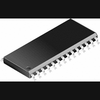
CS8420-CS Cirrus Logic Inc, CS8420-CS Datasheet - Page 73

CS8420-CS
Manufacturer Part Number
CS8420-CS
Description
Transceiver IC
Manufacturer
Cirrus Logic Inc
Datasheet
1.CS8420-CS.pdf
(80 pages)
Specifications of CS8420-CS
Audio Control Type
Sample Rate Converter
Supply Voltage Range
4.75V To 5.25V
Operating Temperature Range
-10°C To +70°C
Audio Ic Case Style
SOIC
No. Of Pins
28
Msl
MSL 2 - 1 Year
Frequency Max
108GHz
Bandwidth
20kHz
Rohs Compliant
No
Lead Free Status / RoHS Status
Contains lead / RoHS non-compliant
Available stocks
Company
Part Number
Manufacturer
Quantity
Price
Company:
Part Number:
CS8420-CS
Manufacturer:
CRY
Quantity:
5 510
Company:
Part Number:
CS8420-CS
Manufacturer:
CIRRUS
Quantity:
225
Part Number:
CS8420-CS
Manufacturer:
CRYSTAL
Quantity:
20 000
Company:
Part Number:
CS8420-CS*
Manufacturer:
NEC
Quantity:
700
Company:
Part Number:
CS8420-CSZ
Manufacturer:
CIRRUS
Quantity:
319
Company:
Part Number:
CS8420-CSZ
Manufacturer:
CIRRUS
Quantity:
9 908
Part Number:
CS8420-CSZ
Manufacturer:
CIRRUS
Quantity:
20 000
Contents of F buffer
Updated from E
Output at Fso rate
The user can configure the interrupt enable register
to cause interrupts to occur whenever “D to E” or
“E to F” buffer transfers occur. This allows deter-
mination of the allowable time periods to interact
with the E buffer.
Also provided are “D to E” and “E to F” inhibit
bits. The associated buffer transfer is disabled
whenever the user sets these bits. These may be
used whenever “long” control port interactions are
occurring. They can also be used to align the be-
havior of the buffers with the selected audio data
flow. For example, if the audio data flow is serial
port in to AES3 out, then it is necessary to inhibit
“D toE” transfers, since these would overwrite the
desired transmit C data with invalid data.
Flowcharts for reading and writing to the E buffer
are shown in Figures 41 and 42. For reading, since
a D to E interrupt just occurred, then there a sub-
stantial time interval until the next D to E transfer
(approximately 192 frames worth of time). This is
usually plenty of time to access the E data without
having to inhibit the next transfer.
DS245PP2
Contents of E buffer
Updated at Fsi rate
Contents of E buffer
Updated at Fsi rate
Contents of F buffer
Updated from E
Output at Fso rate
Figure 41. Flowchart for Reading the E Buffer
D to E interrupt occurs
Return
Optionally set D to E inhibit
If set, clear D to E inhibit
block 1
Figure 40. Channel Status Block Handling When Fso is Not Equal to Fsi
block 1
block 1
Read E data
block 1
block 2
block 1
Fso > Fsi (3/2) Causes blocks 1 and 3 to be transmitted twice
Fso < Fsi (2/3) Causes blocks 3 and 6 to not be transmitted
block 2
block 2
block 3
block 2
For writing, the sequence starts after a E to F trans-
fer, which is based on the output timebase. Since a
D to E transfer could occur at any time (this is
based on the input timebase), then it is important to
inhibit D to E transfers while writing to the E buffer
until all writes are complete. Then wait until the
next E to F transfer occurs before enabling D to E
transfers. This ensures that the data written to the E
buffer actually gets transmitted and not overwritten
by a D to E transfer.
If the channel status block to transmit indicates
PRO mode, then the CRCC byte is automatically
calculated by the CS8420, and does not have to be
written into the last byte of the block by the host
microcontroller.
block 4
block 3
block 3
Figure 42. Flowchart for Writing the E Buffer
block 4
E to F interrupt occurs
Return
block 5
block 3
Optionally set E to F inhibit
If set, clear E to F inhibit
Wait for E to F transfer
block 4
Clear D to E inhibit
Set D to E inhibit
block 5
block 6
Write E data
block 4
block 7
block 5
block 5
CS8420
block 7
73


