AD9551BCPZ Analog Devices Inc, AD9551BCPZ Datasheet - Page 2
AD9551BCPZ
Manufacturer Part Number
AD9551BCPZ
Description
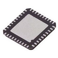
IC, CLOCK GENERATOR, 806MHZ, LFCSP-40
Manufacturer
Analog Devices Inc
Datasheet
1.AD9551PCBZ.pdf
(40 pages)
Specifications of AD9551BCPZ
Clock Ic Type
Clock Generator
Ic Interface Type
SCI
Frequency
806MHz
No. Of Outputs
2
Supply Current
169mA
Digital Ic Case Style
LFCSP
No. Of Pins
40
Lead Free Status / RoHS Status
Lead free / RoHS Compliant
Available stocks
Company
Part Number
Manufacturer
Quantity
Price


AD9551
TABLE OF CONTENTS
Features .............................................................................................. 1
Applications ....................................................................................... 1
General Description ......................................................................... 1
Basic Block Diagram ........................................................................ 1
Revision History ............................................................................... 2
Functional Block Diagram .............................................................. 3
Specifications ..................................................................................... 4
Absolute Maximum Ratings ............................................................ 8
Pin Configuration and Function Descriptions ............................. 9
Typical Performance Characteristics ........................................... 11
Preset Frequency Ratios ................................................................. 14
REVISION HISTORY
9/09—Rev. A to Rev. B
Changes to Table 25 ........................................................................ 33
6/09—Rev. 0 to Rev. A
Changes to Figure 23 ...................................................................... 23
4/09—Revision 0: Initial Version
Reference Clock Input Characteristics ...................................... 4
Output Characteristics ................................................................. 4
Jitter Characteristics (180 Hz Loop Bandwidth) ...................... 5
Crystal Oscillator Characteristics............................................... 5
Power Consumption .................................................................... 5
Logic Input Pins ............................................................................ 6
RESET Pin ..................................................................................... 6
Logic Output Pins ......................................................................... 6
Serial Control Port ....................................................................... 6
Serial Control Port Timing ......................................................... 7
ESD Caution .................................................................................. 8
Rev. B | Page 2 of 40
Theory of Operation ...................................................................... 16
Applications Information .............................................................. 25
Serial Control Port ......................................................................... 26
Register Map ................................................................................... 29
Outline Dimensions ....................................................................... 40
Operating Modes ........................................................................ 16
Component Blocks ..................................................................... 16
Holdover Mode ........................................................................... 21
Jitter Tolerance ............................................................................ 21
External Loop Filter Capacitor ................................................. 21
Output/Input Frequency Relationship .................................... 21
Calculating Divider Values ....................................................... 22
Low Dropout (LDO) Regulators .............................................. 24
Thermal Performance ................................................................ 25
Serial Control Port Pin Descriptions ....................................... 26
Operation of the Serial Control Port ....................................... 26
Instruction Word (16 Bits) ........................................................ 27
MSB/LSB First Transfers ........................................................... 27
Register Map Descriptions ........................................................ 32
Ordering Guide .......................................................................... 40
Related parts for AD9551BCPZ
Image
Part Number
Description
Manufacturer
Datasheet
Request
R

Part Number:
Description:
BOARD EVAL FOR AD9951
Manufacturer:
Analog Devices Inc
Datasheet:


Part Number:
Description:
±1.7g Dual-Axis IMEMS Accelerometer Evaluation Board
Manufacturer:
Analog Devices Inc
Datasheet:

Part Number:
Description:
Inertial Sensor Evaluation System
Manufacturer:
Analog Devices Inc
Datasheet:
Part Number:
Description:
Manufacturer:
Analog Devices Inc
Datasheet:
Part Number:
Description:
Manufacturer:
Analog Devices Inc
Datasheet:
Part Number:
Description:
Manufacturer:
Analog Devices Inc
Datasheet:
Part Number:
Description:
Manufacturer:
Analog Devices Inc
Datasheet:
Part Number:
Description:
Manufacturer:
Analog Devices Inc
Datasheet:
Part Number:
Description:
Manufacturer:
Analog Devices Inc
Datasheet:
Part Number:
Description:
Manufacturer:
Analog Devices Inc
Datasheet:
Part Number:
Description:
Manufacturer:
Analog Devices Inc
Datasheet:
Part Number:
Description:
Manufacturer:
Analog Devices Inc
Datasheet: