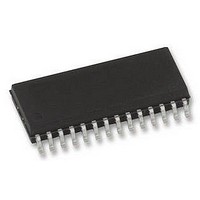
ADC12138CIWM National Semiconductor, ADC12138CIWM Datasheet - Page 29

ADC12138CIWM
Manufacturer Part Number
ADC12138CIWM
Description
IC, ADC, 12BIT, SELF-CALIB, 28SOIC
Manufacturer
National Semiconductor
Datasheet
1.ADC12138CIWM.pdf
(42 pages)
Specifications of ADC12138CIWM
Resolution (bits)
12bit
Input Channel Type
Pseudo Differential, Single Ended
Data Interface
Serial, SPI
Supply Voltage Range - Analogue
3V To 5.5V
Supply Voltage Range - Digital
3V To 5.5V
Sampling Rate
114kSPS
Rohs Compliant
Yes
Lead Free Status / RoHS Status
Lead free / RoHS Compliant
Available stocks
Company
Part Number
Manufacturer
Quantity
Price
Company:
Part Number:
ADC12138CIWMX/NOPB
Manufacturer:
NS
Quantity:
7 504
is the data bit stream required at DI during I/O sequence
number 4 in Figure 8 to set CH1 as the positive input and CH0
as the negative input for the different ADC versions.
Where X can be a logic high (H) or low (L).
1.5 Power Up/Down
The ADC may be powered down by taking the PD pin HIGH
or by the instruction input at DI (see Table 4 and Table 5, and
1.6 User Mode and Test Mode
An instruction may be issued to the ADC to put it into test
mode, which is used by the manufacturer to verify complete
functionality of the device. During test mode CH0–CH7 be-
come active outputs. If the device is inadvertently put into the
test mode with CS continuously low, the serial communica-
tions may be desynchronized. Synchronization may be re-
gained by cycling the power supply voltage to the device.
Cycling the power supply voltage will also set the device into
user mode. If CS is used in the serial interface, the ADC may
be queried to see what mode it is in. This is done by issuing
a “read STATUS register” instruction to the ADC. When bit 9
of the status register is high, the ADC is in test mode; when
bit 9 is low the ADC, is in user mode. As an alternative to
cycling the power supply, an instruction sequence may be
used to return the device to user mode. This instruction se-
quence must be issued to the ADC using CS. The following
table lists the instructions required to return the device to user
mode. Note that this entire sequence, including both Test
Mode and User Mode values, should be sent to recover from
the test mode.
ADC12130
ADC12132
ADC12138
Number
Part
and
DI0 DI1 DI2 DI3 DI4 DI5 DI6 DI7
L
L
H
H
L
L
FIGURE 8. Changing the ADC's Conversion Configuration
DI Data
L
L
H
L
L
L
H
X
X
L
29
the Power Up/Down timing diagrams). When the ADC is pow-
ered down in this way, the ADC conversion circuitry is deac-
tivated but the digital I/O circuitry is kept active.
Hardware power up/down is controlled by the state of the PD
pin. Software power-up/down is controlled by the instruction
issued to the ADC. If a software power up instruction is issued
to the ADC while a hardware power down is in effect (PD pin
high) the device will remain in the power-down state. If a soft-
ware power down instruction is issued to the ADC while a
hardware power up is in effect (PD pin low), the device will
power down. When the device is powered down by software,
it may be powered up by either issuing a software power up
instruction or by taking PD pin high and then low. If the power
down command is issued during a conversion, that conver-
sion is interrupted, so the data output after power up cannot
be relied upon.
X = Don't Care
The power up, data with or without sign, and acquisition time
instructions should be resent after returning to the user mode.
This is to ensure that the ADC is in the required state before
a conversion is started.
Set Acquisition
Set DO with or
USER MODE
TEST MODE
without Sign
Instruction
Instructions
Conversion
Test Mode
Power Up
Start a
Reset
Time
H or
H or
H or
DI0 DI1 DI2 DI3 DI4 DI5 DI6 DI7
H
L
L
L
L
L
L
L
L
H or
H or
X
L
L
L
L
L
L
L
L
H or
X
L
L
L
L
L
L
L
L
H or
DI Data
X
L
L
L
L
L
L
L
L
H
H
H
H
H
H
H
H
L
H or
H
H
H
H
H
1207933
L
L
L
L
www.national.com
H or
H
H
H
H
H
H
H
L
L
H or
H
H
H
H
L
L
L
L
L


