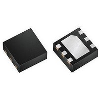
LT3491EDC#PBF Linear Technology, LT3491EDC#PBF Datasheet - Page 11

LT3491EDC#PBF
Manufacturer Part Number
LT3491EDC#PBF
Description
IC, LED DRVR, DFN6
Manufacturer
Linear Technology
Datasheet
1.LT3491EDCPBF.pdf
(16 pages)
Specifications of LT3491EDC#PBF
Led Driver Application
Mobile Phone Display Lighting, General LED Lighting
No. Of Outputs
1
Output Current
200mA
Output Voltage
32V
Input Voltage
2.5V To 12V
Dimming Control Type
PWM
Topology
Boost (Step Up)
Rohs Compliant
Yes
Lead Free Status / RoHS Status
Lead free / RoHS Compliant
Available stocks
Company
Part Number
Manufacturer
Quantity
Price
APPLICATIO S I FOR ATIO
LOW INPUT VOLTAGE APPLICATIONS
The LT3491 can be used in low input voltage applications.
The input supply voltage to the LT3491 must be 2.5V or
higher. However, the inductor can be run off a lower
battery voltage. This technique allows the LEDs to be
powered off two alkaline cells. Most portable devices have
a 3.3V logic supply voltage which can be used to power the
LT3491. The LEDs can be driven straight from the battery,
resulting in higher efficiency.
Figure 10 shows three LEDs powered by two AA cells. The
battery is connected to the inductor and the chip is
powered off a 3.3V logic supply voltage.
(A) SC70 PACKAGE
LED
R
SENSE
CTRL
U
CAP
U
C
OUT
V
5
6
7
8
IN
C
IN
2 AA CELLS
2V TO 3.2V
W
GND
GND
3.3V
Figure 11. Recommended Component Placement
0.1µF
Figure 10. 2 AA Cells to Three White LEDs
4
3
2
1
C1
U
C1: TAIYO YUDEN LMK212BJ105MD
C2: TAIYO YUDEN GMK325BJ225ML
L1: MURATA LQH32CN100
C1
1µF
10µH
SW
L1
L1
DIMMING CONTROL
V
SW
SHUTDOWN AND
IN
LT3491
CTRL
GND
BOARD LAYOUT CONSIDERATIONS
As with all switching regulators, careful attention must be
paid to the PCB board layout and component placement.
To prevent electromagnetic interference (EMI) problems,
proper layout of high frequency switching paths is essen-
tial. Minimize the length and area of all traces connected to
the switching node pin (SW). Keep the sense voltage pins
(CAP and LED) away from the switching node. Place C
next to the CAP pin. Always use a ground plane under the
switching regulator to minimize interplane coupling. Rec-
ommended component placement is shown in Figure 11.
CAP
LED
(B) DFN PACKAGE
SW
V
IN
L1
R
10Ω
C
SENSE
IN
3491 F10
1
2
3
C2
2.2µF
GND
7
C
6
5
4
OUT
CTRL
CAP
LED
R
SENSE
LT3491
3491 F11
11
3491fa
OUT


