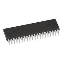
MAX6952EPL+ Maxim Integrated Products, MAX6952EPL+ Datasheet - Page 11

MAX6952EPL+
Manufacturer Part Number
MAX6952EPL+
Description
LED Driver IC
Manufacturer
Maxim Integrated Products
Specifications of MAX6952EPL+
Operating Temperature Range
-40°C To +85°C
Driver Case Style
DIP
Peak Reflow Compatible (260 C)
Yes
Device Type
LED
Display Interface
Common Cathode, Multiplexed
Termination Type
Through Hole
Filter Terminals
Through Hole
Rohs Compliant
Yes
Led Display Type
Dot Matrix / Graphic
Lead Free Status / RoHS Status
Lead free / RoHS Compliant
When blink is globally disabled, then only the digit data
in plane P0 is used to control the display. The digit data
in plane P1 is ignored.
By setting the T bit in multiple MAX6952s at the same
time (or in quick succession), the blink timing can be
synchronized across all the devices (Table 11). Note
that the display multiplexing sequence is also reset,
which might give rise to a one-time display flicker when
the register is written.
When global digit data clear is set, the digit data for both
planes P0 and P1 for all digits is cleared (Table 12).
Figure 6. MAX6952 Daisy-Chain Connection
Table 8. Blink Rate Selection (B Data Bit D2) Format
Table 9. Global Blink Enable/Disable (E Data Bit D3) Format
Blink function is disabled.
Blink function is enabled.
Slow blinking (Segments are refreshed using plane P0 for 1s, plane P1
for 1s, for OSC = 4MHz.)
Global Clear Digit Data (R Data Bit D5) Format
MICROCONTROLLER
MODE
Global Blink Timing Synchronization
______________________________________________________________________________________
DOUT
CLK
DIN
CS
4-Digit 5
MODE
(T Data Bit D4) Format
DIN
CLK
CS
D7
MAX6952
P
P
4-Wire Interfaced, 2.7V to 5.5V,
✕
DOUT
D6
7 Matrix LED Display Driver
X
X
D5
R
R
When the configuration register is read, the P bit
reflects the state of the blink output pin at that time
(Table 13).
The font is a 5
ROM, and 24 user-definable characters. The selection
from the total of 128 characters is represented by the
lower 7 bits of the 8-bit digit registers. The most-signifi-
cant bit, shown as x in the ROM map below, is zero to
light LEDs as shown by the black segments in Table
14, and 1 to display the inverse.
The character map follows the Arial font for 96 charac-
ters in the x0101000 through x1111111 range. The first
DIN
CLK
CS
MAX6952
Blink Phase Readback (P Data Bit D7) Format
REGISTER DATA
D7
P
D4
T
T
Character Generator Font Mapping
DOUT
D6
X
✕
7 matrix comprising 104 characters in
D3
D5
0
1
R
REGISTER DATA
D4
DIN
CLK
T
CS
D2
B
B
MAX6952
D3
E
D2
0
D1
DOUT
X
X
D1
X
D0
S
S
D0
S
11


