CAT4004VP2-T3 CATALYST SEMICONDUCTOR, CAT4004VP2-T3 Datasheet
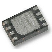
IC, LED DRIVER, CONSTANT CURRENT, TDFN-8

CAT4004VP2-T3

Manufacturer Part Number
CAT4004VP2-T3
Description
IC, LED DRIVER, CONSTANT CURRENT, TDFN-8
Manufacturer
CATALYST SEMICONDUCTOR
Datasheet

Specifications of CAT4004VP2-T3

Led Driver Application
LCD Display Backlight, Digital Still Cameras
No. Of Outputs
4
Output Current
40mA
Output Voltage
3.3V
Input Voltage
2.4V To 5.5V
Topology
Constant Current
Lead Free Status / RoHS Status
Lead free / RoHS Compliant
CAT4004
4-Channel Constant Current
LED Driver with EZDimt
Description
drive LEDs. An external resistor on RSET sets the current in the LED
channels. Each LED channel includes an individual control loop
allowing the device to handle a wide range of LED forward voltages
while still maintaining tight current matching.
dimming interface for current setting of all LEDs. Six different current
dimming ratios are available.
required that the battery or voltage source have enough headroom to
drive the LED forward voltage and current sink (>150 mV).
package with a max height of 0.8 mm.
Features
Applications
© Semiconductor Components Industries, LLC, 2010
March, 2010 − Rev. 2
programming
The CAT4004 provides four matched low dropout current sources to
The EN/DIM logic inputs supports device enable and a digital
The device is aimed at “direct drive” battery applications. It is
The device is available in a tiny 8−lead TDFN 2 mm x 3 mm
Compliant
Four LED Current Sinks with Tight Matching
Low Dropout Driver 130 mV at 30 mA
No Switching Noise
Shutdown Current < 1 mA
LED Current set by External Resistor
Dimming via 1−wire EZDimt Interface
Thermal Shutdown Protection
8−lead 2 mm x 3 mm TDFN Package
These Devices are Pb−Free, Halogen Free/BFR Free and are RoHS
LCD Display Backlight
Cellular Phones
Digital Still Cameras
Handheld Devices
2.4 V
5.5 V
V
IN
to
One wire
3.8 kW
Figure 1. Typical Application Circuit
RSET
C
1 mF
IN
VIN
EN/DIM
RSET
LED1 LED2 LED3 LED4
CAT4004
GND
20 mA
1
CAT4004VP2−T3
(Note 1)
CAT4004VP2−GT3
(Note 2)
1. Matte−Tin Plated Finish (RoHS−compliant).
2. NiPdAu Plated Finish (RoHS−compliant).
FX = CAT4004VP2−T3
HA = CAT4004VP2−GT3
A = Assembly Location
XXX = Last Three Digits of Assembly Lot Number
Y = Production Year (Last Digit)
M = Production Month (1−9, A, B, C)
EN/DIM
Device
LED1
LED2
GND
ORDERING INFORMATION
XXX
FXA
MARKING DIAGRAMS
YM
PIN CONNECTIONS
http://onsemi.com
CASE 511AK
VP2 SUFFIX
1
(Top View)
TDFN−8
(Pb−Free)
(Pb−Free)
Package
TDFN−8
TDFN−8
Publication Order Number:
HAA
XXX
VIN
RSET
LED4
LED3
Tape & Reel
Tape & Reel
YM
Shipping
3,000/
3,000/
CAT4004/D

Related parts for CAT4004VP2-T3

CAT4004VP2-T3 Summary of contents

Page 1

... March, 2010 − Rev. 2 http://onsemi.com PIN CONNECTIONS EN/DIM GND LED1 LED2 MARKING DIAGRAMS FXA XXX CAT4004VP2− CAT4004VP2−GT3 A = Assembly Location XXX = Last Three Digits of Assembly Lot Number Y = Production Year (Last Digit Production Month (1− ORDERING INFORMATION Device CAT4004VP2− (Note 1) CAT4004VP2− ...

Page 2

Table 1. ABSOLUTE MAXIMUM RATINGS VIN, LEDx, RSET EN/DIM Voltage Storage Temperature Range Junction Temperature Range Lead Temperature Stresses exceeding Maximum Ratings may damage the device. Maximum Ratings are stress ratings only. Functional operation above the Recommended Operating Conditions is ...

Page 3

Table 4. RECOMMENDED EN/DIM TIMING (For 2.4 ≤ V ≤ 5.5 V, over full ambient temperature range −40°C to +85°C.) IN Symbol Name T EN/DIM setup from shutdown SETUP T EN/DIM program low time LO T EN/DIM program high time ...

Page 4

TYPICAL PERFORMANCE CHARACTERISTICS ( 3 LEDs OUT 1.4 1.2 1.0 0.8 0.6 2.5 3.0 3.5 4.0 INPUT VOLTAGE (V) Figure 3. Quiescent Current ...

Page 5

TYPICAL PERFORMANCE CHARACTERISTICS ( 3 LEDs OUT 0.7 0.6 0.5 0.4 0.3 0.2 2.0 2.5 3.0 3.5 4.0 INPUT VOLTAGE (V) Figure 8. ...

Page 6

TYPICAL PERFORMANCE CHARACTERISTICS ( 3 LEDs OUT Figure 13. Power Up Waveform Figure 15. Line Transient Waveform 5 ...

Page 7

Table 5. PIN DESCRIPTIONS Pin # Name 1 EN/DIM Device enable (active high) and dimming control 2 GND Ground reference 3 LED1 LED1 cathode terminal 4 LED2 LED2 cathode terminal 5 LED3 LED3 cathode terminal 6 LED4 LED4 cathode terminal ...

Page 8

Block Diagram V IN VIN RSET EN/DIM Figure 17. CAT4004 Functional Block Diagram Basic Operation The CAT4004 uses four tightly matched current sinks to accurately regulate LED current in each channel proportional to the current sourced from the RSET pin. ...

Page 9

D E PIN#1 INDEX AREA TOP VIEW SYMBOL MIN NOM A 0.70 0.75 A1 0.00 0.02 A2 0.45 0.55 A3 0.20 REF b 0.20 0.25 D 1.90 2.00 D2 1.30 1.40 E 2.90 3.00 E2 1.20 1.30 e 0.50 TYP ...

Page 10

... All packages are RoHS−compliant (Lead−free, Halogen−free). 5. The standard lead finish is NiPdAu. 6. The device used in the above example is a CAT4004VP2−GT3 (TDFN, NiPdAu Plated Finish, Tape & Reel, 3,000/Reel). 7. For Matte−Tin package option, please contact your nearest ON Semiconductor Sales office. ...

Related keywords