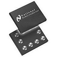
LM3502SQ-25/NOPB National Semiconductor, LM3502SQ-25/NOPB Datasheet - Page 5

LM3502SQ-25/NOPB
Manufacturer Part Number
LM3502SQ-25/NOPB
Description
IC, WHITE LED DRIVER, BOOST, LLP-10
Manufacturer
National Semiconductor
Datasheet
1.LM3502SQ-35NOPB.pdf
(18 pages)
Specifications of LM3502SQ-25/NOPB
Led Driver Application
Display Backlighting, Cellular Phones And PDAs
No. Of Outputs
2
Output Current
600mA
Output Voltage
24.5V
Input Voltage
2.5V To 5.5V
Topology
Boost
Lead Free Status / RoHS Status
Lead free / RoHS Compliant
I
I
UVP
OVP
V
V
V
T
I
I
V OUT1
V OUT2
En1
En2
Symbol
SHDW
En1
En2
Cntrl
Preliminary Electrical Characteristics
Limits in bold typeface apply over the full operating junction temperature range (−40˚C ≤ T
specified, V
Note 1: Absolute maximum ratings indicate limits beyond which damage to the device may occur. Electrical characteristic specifications do not apply when
operating the device outside of its rated operating conditions.
Note 2: The human body model is a 100 pF capacitor discharged through a 1.5 kΩ resistor into each pin. The machine model is a 200 pF capacitor discharged
directly into each pin.
Note 3: Current flows into the pin.
Note 4: The maximum allowable power dissipation is a function of the maximum junction temperature, T
and the ambient temperature, T
calculated using: P
on this topic, please refer to Application Note 1187: Leadless Leadframe Package (LLP) and Application Note 1112 (AN1112) for microSMD chip scale package.
Note 5: The on threshold indicates that the LM3502 is no longer switching or regulating LED current, while the off threshold indicates normal operation.
Note 6: All voltages are with respect to the potential at the GND pin.
Note 7: Min and Max limits are guaranteed by design, test, or statistical analysis. Typical numbers are not guaranteed, but do represent the most likely norm.
Note 8: Current flows out of the pin.
(ON) V
Current (Note 3)
V
Current (Note 3)
Under-Voltage
Protection
Over-Voltage
Protection (Note 5)
PMOS FET Switch
Enabling Threshold
(Figure 2: P1)
NMOS FET Switch
Enabling Threshold
(Figure 2: N2)
Device Enabling
Threshold
Shutdown Delay Time
En1 Pin Input Bias
Current
En2 Pin Input Bias
Current
IN
OUT1
OUT2
= 2.5V. (Continued)
D
(MAX) = (T
Parameter
Pin Bias
Pin Leakage
J
(MAX) – T
A
. See Thermal Properties for the thermal resistance. The maximum allowable power dissipation at any ambient temperature is
A
)/θ
V
V
V
V
Fb = 0V, Cntrl = 0V, V
On Threshold
Off Threshold
On Threshold (16)
Off Threshold (16)
On Threshold (25)
Off Threshold (25)
On Threshold (35)
Off Threshold (35)
On Threshold (44)
Off Threshold (44)
Off Threshold (Display Lighting)
On Threshold (Display Lighting)
Off Threshold (Display Lighting)
On Threshold (Display Lighting)
Off Threshold
OnThreshold
En1 = 2.5V
En1 = 0V
En2 = 2.5V
En2 = 0V
OUT1
OUT1
OUT1
OUT1
JA
. Exceeding the maximum allowable power dissipation will cause excessive die temperature. For more information
= 14V, Cntrl = 1.5V (16)
= 23V, Cntrl = 1.5V (25)
= 32V, Cntrl = 1.5V (35)
= 42V, Cntrl = 1.5V (44)
Conditions
OUT2
(Notes 6, 7) Limits in standard typeface are for T
= 42V
5
J
(MAX), the junction-to-ambient thermal resistance, θ
14.5
14.0
22.5
21.5
32.0
31.0
40.5
39.0
Min
2.2
1.4
1.4
1.4
8
J
≤ +125˚C). Unless otherwise
15.5
Typ
0.1
2.4
2.3
0.8
0.8
0.8
0.8
0.8
0.8
0.1
0.1
40
50
50
85
15
24
23
34
33
42
41
12
7
7
Max
16.5
16.0
25.5
24.5
35.0
34.0
43.5
42.0
100
100
140
2.5
0.3
0.3
0.3
80
16
14
14
3
J
= 25˚C.
www.national.com
Units
ms
µA
µA
µA
µA
V
V
V
V
V
JA
,


